Device overview
|
|
|
|
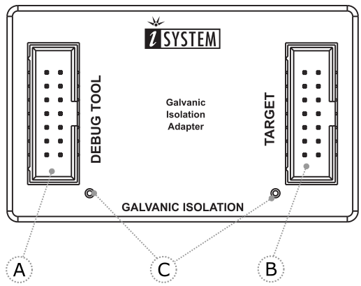
A – DEBUG TOOL connector.
B – TARGET connector.
C – LED lights indicate power supply status.
|
If LEDs on the GI Adapter are OFF, immediately turn everything OFF! |

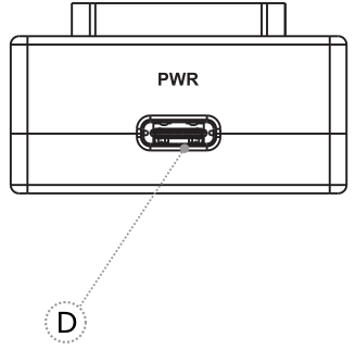
D – USB PD Power supply socket (PWR).
|
Use only original USB PD Power supply for powering and connecting with the GI Adapter, otherwise the primary functionality of the GI Adapter would be counteracted. |
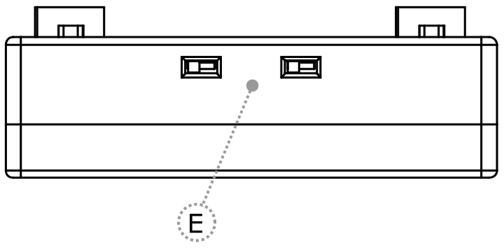
E – Debug interface (SWD, JTAG) selection.
Both jumpers (SW1, SW2) should be in the same position to achieve the desired debug interface. The legend is printed on the housing.
Debug interface |
SW1 |
SW2 |
||||
|---|---|---|---|---|---|---|
SWD |
|
|
||||
JTAG |
|
|
Pinout
10-pin 1.27 mm CoreSight Debug Adapter
The following pinout is valid on the target side:
Signal Direction |
Signal Description |
Signal |
Pin |
Pin |
Signal |
Signal Description |
Signal Direction |
|---|---|---|---|---|---|---|---|
I |
Reference Voltage |
Vref |
1 |
2 |
SWDIO/TMS |
SWD/JTAG |
I/O / O |
|
Ground |
GND |
3 |
4 |
SWCLK/TCK |
SWD/JTAG |
O |
|
Ground |
GND |
5 |
6 |
SWO/TDO |
SWD/JTAG |
I |
|
Not Connected |
KEY |
7 |
8 |
NC/TDI |
Not Connected /JTAG |
O |
|
Ground |
GND |
9 |
10 |
nRESET |
Reset |
I/O |
10-pin ARM CoreSight pinout
20-pin 1.27 mm CoreSight Debug Adapter
The following pinout is valid on the target side:
Signal Direction |
Signal Description |
Signal |
Pin |
Pin |
Signal |
Signal Description |
Signal Direction |
|---|---|---|---|---|---|---|---|
I |
Reference Voltage |
Vref |
1 |
2 |
SWDIO/TMS |
JTAG |
I/O / O |
|
Ground |
GND |
3 |
4 |
SWCLK/TCK |
JTAG |
O |
|
Ground |
GND |
5 |
6 |
SWO/TDO |
JTAG |
I |
|
Not Connected |
KEY |
7 |
8 |
NC/TDI |
Not Connected / JTAG |
O |
|
Ground |
GND |
9 |
10 |
nRESET |
Reset |
I/O |
|
Reference Voltage/Ground |
NC_CAPGND |
11 |
12 |
NC |
Not Connected |
|
|
Reference Voltage/Ground |
NC_CAPGND |
13 |
14 |
NC |
Not Connected |
|
|
Ground |
GND |
15 |
16 |
NC |
Not Connected |
|
|
Ground |
GND |
17 |
18 |
NC |
Not Connected |
|
|
Ground |
GND |
19 |
20 |
NC |
Not Connected |
|
20-pin Arm CoreSight pinout