Debugging dialog reference
Select Hardware > SoC Options > Debugging.
|
This dialog allows Infineon TriCore SCR debugging via Private DAP. |

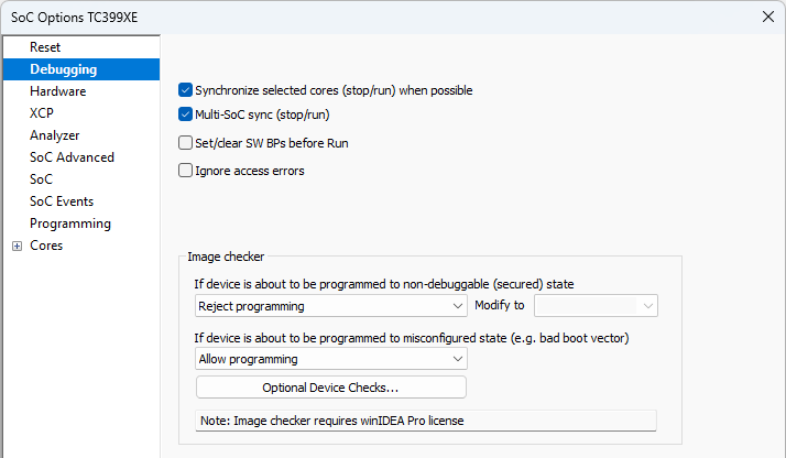
Debugging page of SoC Options dialog (architecture-specific)
Synchronize selected cores (stop/run) when possible
Checked option configures available on-chip debug logic for cores to stop and run at the same time when debugging. If you want to a specific core to be included in the synchronization, it must be enabled in the Cores > core > Synchronize this core option as well.
Note that all synchronization combinations might not be possible. The possibilities are determined by the target architecture, synchronization resources, SoC restrictions, etc.
Refer to the reference manuals and descriptions of used architecture and SoC for more information.
This option is not applicable for RH850. All cores are always synced.
Set/clear SW BPs before Run
When the option is checked, then a software breakpoint is not set / cleared immediately, but is just remembered. Only when the SoC is set to running are the breakpoints committed. This way several breakpoints can be changed but only one re-FLASH operation takes place. This is especially noticeable in testIDEA operation with many stubs and also during a regular debugging session when several breakpoints are set / cleared within the same flash erase block.
Ignore access errors
When checked, the debugger identifies memory access errors for individual memory location(s). When the option is unchecked, the debugger would declare access error for remaining memory locations once one access error is detected within a memory read block, which is used in the Disassembly Window or Memory Window.
Enable low power mode debug (on supported devices only)
Select this option to enable the debugger synchronization algorithm for devices that support a low power mode entry and exit debugger synchronization mechanism.
Image checker (SoC-dependent)
Supported for
•Infineon AURIX TC2xx, TC3xx)
•MPC56xx and SPC58
Image checker analyzes the program file(s) at program to prevent misconfiguration of SoC, which could result in incorrect boot or bricked SoC due to disabled debug periphery. It distinguishes between:
•non-debuggable (secured) state - Destructive violations after which SoC would not be useful anymore due to disabled debug
•non-destructive violations (e.g. bad Boot vector)
Each class of violations has three options:
•Allow programming - executes program
•Modify write data to keep device unsecured - winIDEA tries to patch program data with correct values. If it is not possible, the operation is rejected
•Reject programming - prevents program
|
HSM boot vector on TriCore is treated as a destructive violation. |
winIDEA displays a warning in the Progress window about:
•a warning if Patch is applied or
•an error if programming is rejected
•Session initialization will fail if programming is rejected
When Reject policy is selected, the warning becomes an error message and operation is aborted. Same happens when Modify is selected, but the configuration cannot be fixed automatically.
Optional Device Checks
Select optional image checks available before flash programming.
Option Checks Program entry in Optional Device Checks checks if the program entry address is reachable. Entry point is considered as specified in the default symbol file, unless overridden in Hardware > SoC Options > Cores | Address (Preset PC after stopped in init).
Architecture-specific options
Arm Cortex-specific
CPU clock
Set this to core clock. It might be used internal FLASH programming timing, depending on the SoC that is being used. When it is used for both set to core clock valid when trace is active then use initialization sequence to set the SoC clock the same frequency for programming.
|
Note that this setting is critical to FLASH operations on many SoCs. |

If flash programming fails, check if this setting is correct. This setting must be valid at the moment when flash programming is performed. When the application is first programmed the SoC runs on the default clock (out of reset). This means that the clock setting must be correct at the time of program. If you wish to use software breakpoints / write to flash once the SoC clock is changed (e.g. PLLs are used), then it is necessary to set this setting to the clock that is valid at this time and create a winIDEA initialization script that will set the SoC clock to the same frequency prior to application program. This ensures that the SoC clock setting is valid both at the time of the application program and later on as well. Refer to Initialization Sequence for more information.
Example
50 MHz is entered as SoC clock:
a.SoC runs on 12MHz out of reset (program will not work)
b.Initialization script sets the SoC clock to 50MHz
c.Program is performed
d.SoC is reset (clock is reset back to 12MHz) – if Reset SoC after DL/reset option is enabled
e.Flash operations / trace unoperable until the clock is set to 50MHz by the application
|
This might not be necessary on all Cortex devices, but most Cortex-M NXP LPC devices need SoC clock to correctly program FLASH memory. |
Simulate instr. step
Never is selected by default. When run or source step debug command is executed from a BP location the debugger first clears BP, executes single step, sets back the original BP and then resumes the application. All this is done in background hidden from the user. Since setting and clearing software flash breakpoint can be very time consuming the new approach was introduced. It simulates the first instruction at breakpoint address without clearing and setting the software flash breakpoint. Thereby the user can select FLASH SW BP in order to speed up the debugging. Not all instructions can be simulated successfully. If the option yields erroneous behavior, set back to the default setting.
Renesas RH850-specifics
External Oscillator Clock
Enter the frequency of the external quartz oscillator connected to the target SoC. This value is used when performing the Renesas native FP5 serial protocol operations in Python scripts.
Ignore access errors
Any access to an undefined address space or non-initialized internal RAM returns an error status. This is displayed with question marks ‘?’ all over the memory window when such an address base is given.
Nevertheless, to be able to inspect the state of the internal RAM check this option, and set the RAM Initialization option to Never in the Reset page.
Infineon TriCore specifics
Debug channel (cable connection)
You can configure the settings for debugging the SCR SoC via Private DAP. Make sure you select a suitable DAP or SPD (Single Pin DAP) according to your application and target pin out. Note that SPD is not supported on the iC5000 BlueBox.
In case you selected the DAP Debug channel you have to configure the Debug clock as well.
NXP/ST Power architecture specifics
Low Power Mode Debug
Enables the synchronization of entry to and exit from low power mode with the debugger.
This option is only needed on certain microcontrollers, where the debug module is powered off on entry to Low Power Mode. When the option is disabled, winIDEA will lose debug connection to the SoC when low power mode is entered. To ensure a normal debug experience it should be enabled on such SoCs, e.g.: MPC551x, MPC560xB, MPC560xP, MPC560xS, MPC567xK, MPC5668x, MPC564xA, MPC564xL, MPC564xR, SPC56EL70, MPC562xA, MPC574xx (Calypso, Calypso 3M).
Run after low power mode exit
If enabled, the core that wakes up after a low-power mode exit (generally stopped) runs automatically.
Allow access to unimplemented registers
When this option is checked, the debugger will allow access to the core registers (SPRs, PMRs, DCRs), which are not directly supported yet by winIDEA SFRs window.
Possible use case would be if the customer finds a core register, which is not listed yet in the SFRs window. By checking this option and addressing this missing core register in the watch window, user gets immediate access to this register before winIDEA fix is provided.
Note that if you try to access unimplemented core registers, the SoC may hang. Therefore, use this option with caution.