Hardware Design Guidelines
In this topic:
•Test and Debugger integration
Introduction
This note describes guidelines for the SoC hardware design to ensure the correct operation of TASKING debug and trace tools.
Key points
•Connect a debug connector to the SoC debug port and RESET line directly.
•Have a jumper to disable a watchdog timer.
•Consult with the debugger vendor.
•Keep lines short and point-to-point.
•Line-length matching on fast parallel buses.
•Maintain the impedance for both single-ended (50 Ω) and differential signal lines (100 Ω).
•Consider signal crosstalk issues.
•For debugger integration have SoC scripts ready for accessing RAM and FLASH memory.
•Don’t use sockets.
•Use a target connector with a frame and strain relief to minimize the risk of misalignment or reversed connection to the target.
•Do not use any additional adapters between the debug adapter and the target.
•Don’t use nail beds.
Keep reading
The quality of debug and trace signals depends primarily on the implementation of the I/O drivers on the SoC. But even more so on the hardware design itself (circuit diagram and PCB layout). High signal integrity requires careful hardware design to minimize potential integration issues between the SoC and the test equipment.
Furthermore, a production company must verify that its manufactured electronic assemblies pass functional tests. Functional tests always involve JTAG boundary scan tests and running module tests on the SoC at full speed.
The purpose of the following recommendations is to bridge the gap between design, development and production verification steps.
Design recommendations
Modern SoCs share their JTAG pins between the boundary scan registers and the internal debugging unit. Naturally, it's tempting to connect all SoCs with JTAG on the board in a single boundary scan chain. Unfortunately, this too often leads to various problems.
The key point to remember is that not all SoCs are created equal. They are manufactured with different silicon process technologies. Consequently, the fastest components, typically SoCs, RAM, and programmable logic circuits, are more susceptible to JTAG signal interference than other components in the chain.
Schematics
From the very beginning of the design process, the following points must be addressed:
•Have a debug connector for the SoC.
•Use standard target connectors, pinout, and types
oFor more information regarding the target connector and adapter compatibility, consult with TASKING and refer to vendor manuals.
oPlace pull-up and pull-down resistors as defined by SoC and debugger vendors.
•Note that custom adapters degrade debugging performance.
•Have separated JTAG chains for:
oSoC
oprogrammable logic
oother SoCs.
•Make sure the SoC debug port and the RESET line are connected directly to the debug connector.
•Configure the processor pins so that it can boot from a reset without requiring preprogramming of external logic.
•Adjust line termination to I/O driver strength to match trace line impedance.
oPlace the series termination resistor as close as possible to the driver.
oPut AC coupling capacitors as specified by the SoC vendor. They are typically placed as close as possible to the receiver pins, except for the clock output, where they are placed on the driver side for protection.
•Any additional component on a signal line reduces signal quality.
oTherefore, minimize parasitic elements.
•Don’t use debug or trace pins to drive other peripherals.
•Add a jumper to easily disable the board’s watchdog timer.
PCB Layout
Placement
•Place the debug/trace connector as close as possible to the SoC. All JTAG SoC debug and trace lines on the PCB should be as short as possible.
•Do not place tall components near the debug connector to ensure proper connection of the debug probe.
•For best signal integrity, the SoC should be soldered directly to the PCB; any sockets in between degrade performance.
Routing
•If the debug and trace lines are buffered, they must be terminated in series with 50 Ω resistors placed at the driver end. The resistor may vary depending on the driver's specification.
•Connect ground pins directly to the ground plane.
•Route the TCK, the debug and test clock, with double distance to its closest nets. It may cause interference, but it may also be susceptible to noise from other signals.
•The TCK clock path should be a point-to-point connection, free from stubs.
•It is strongly recommended that other (data) lines also be point-to-point, without stubs. If any stubs are needed, they should be as short as possible. If longer segments are required, there should be a possibility to disconnect them.
•Potential crosstalk issues must be considered. Trace port data bus crosstalk is less critical, but it is essential to isolate the entire bus from other signals and pay close attention to the trace clock routing. Keep all trace lines away from potential interfering signals and maintain a minimum distance of three times the trace width from other signals, as the clock itself can interfere with the signal.
•Use the same reference layer - the ground plane is preferred. Check the return signal path, as noise can also appear on the reference plane. If you switch layers, also add return path vias.
•The length of the high-speed parallel bus lines must be matched to ensure that all signals arrive within the receiver's synchronization window.
•Minimize the number of vias. If minimizing is not possible, remember to include return path vias.
•Maintain the impedance of the single-ended (50 Ω) and differential signal lines (100 Ω).
oPlace the series termination resistor as close as possible to the driver.
oFor differential signal pairs, match trace lengths and maintain symmetrical routing to preserve phase alignment. Use the recommended AC-coupling capacitors—typically 100 nF in 0402 SMD packages—to minimize pad discontinuities (stubs). Place the capacitors as close as possible to the receiver pins. For clock outputs, place the capacitor on the driver side for protection. Note that some SoC suppliers may recommend placing all AC-coupling capacitors at the transmitter end.
Test and Debugger integration
•Developers should provide initialization instructions and scripts for accessing the SoC, including pre-initialized CPLDs to drive the reset logic, and specify whether the board requires an external clock, watchdog timer settings, etc.
•Provide initialization scripts for accessing RAM, FLASH memory, and other peripherals. Finally, provide test code for module tests, such as Ethernet loopback tests.
Application guideline
User application software must not reconfigure the debug or trace pins for its own purposes. This allows a debugging tool to retain control of a SoC debug unit and have the possibility to perform program and data tracing as soon as the SoC is released from reset.
When using a parallel trace, always perform a trace line calibration whenever any trace-related parameters are modified, including prescaler, data width, data rate, or sampling point, to ensure signal integrity and timing accuracy.
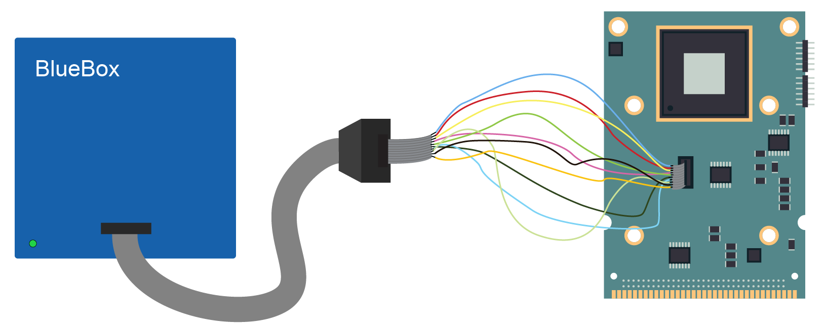
Improvisations
Sometimes the boards are not equipped with a standard debug connector, forcing users to improvise, which too often leads to the very problems addressed above. If you are forced to use improvised wiring, please contact TASKING. We can offer you a customized adapter solution.
If you decide to do it yourselves, we recommend using a flat cable and separate the signals with ground lines. Ensure that leads are as short as possible, less than 25 mm (1 inch).
When contacting TASKING technical support, always mention that you are using custom cabling.
If wiring between a debugger and your target board looks like this, the connection will fail or be unstable.
Conclusion
These hardware design guidelines are intended to support the development of reliable SoC boards with the help of TASKING debugger tools.
By respecting appropriate design margins, and early consideration of manufacturing and testing constraints, these practices reduce risk and improve the design considerably. Trade-offs between performance, cost, and robustness are inevitable, but a disciplined application of these principles helps ensure that integration with a debugger runs smoothly.
Ultimately, these guidelines should serve as both a reference and a framework supporting design reviews, guiding new development, and evolving as technologies and requirements change. When applied thoughtfully, they help transform individual design choices into reliable, high-quality hardware systems.