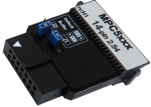
14-pin MPC5xxx (2.54mm) Debug Adapter
This debug adapter is used to connect the BlueBox to the MPC5xxx/SPC5 based target. It’s used to connect to the embedded target featuring a 14-pin 2.54mm pitch target debug connector with the MPC5xxx/SPC5 pinout.
The debug adapter connects to the 25 cm 40-pin ribbon cable coming from the BlueBox and to the target debug connector on the other side.
The following pinout is valid on the target side:
Signal Direction |
Signal Description |
Signal |
Pin |
Pin |
Signal |
Signal Description |
Signal Direction |
|---|---|---|---|---|---|---|---|
O |
JTAG |
TDI |
1 |
2 |
GND |
Ground |
|
I |
JTAG |
TDO |
3 |
4 |
GND |
Ground |
|
O |
JTAG |
TCK |
5 |
6 |
GND |
Ground |
|
O |
Nexus Event Input |
nEVTI(EVTI0) |
7 |
8 |
PORST |
Power On Reset |
I/O |
I/O |
Reset |
nRESET |
9 |
10 |
TMS |
JTAG |
O |
I |
Reference Voltage |
Vref |
11 |
12 |
GND |
Ground |
|
|
Not Connected |
NC |
13 |
14 |
JCOMP |
JTAG TRST (optional) |
O |
14-pin MPC5xxx & SPC5 target pinout
Signal Direction is described from the BlueBox perspective.
|
When initially connecting the BlueBox to a target, ensure the debug adapter pinout matches the Target connector to avoid potential hardware failure. |
14-pin 2.54mm MPC5xxx Debug Adapter features resettable fuses on all connected pins. These protect debug signals against overcurrent and cycle back to a conductive state after the excessive current fades away.
Mandatory pins on the microcontroller side are the GND, Vref, nRESET, TMS, TDI, TDO and TCK.
|
Pin 8 (Power on reset) is supported with the debug adapter C1 or newer. |
The JCOMP is an optional pin. Some microcontrollers don’t have this pin. Internally, this is actually the JTAG TRST, which resets the JTAG TAP state machine. Because the JTAG TAP state machine can be reset also by the TMS and the TCK, this pin is optional also for the debugger. If the microcontroller has the JCOMP pin but it is not connected to the target debug connector, it must be set to the non-active state in the target via a pull-up resistor. If not, then the JTAG TAP state machine remains in reset and debugging is not possible.
Jumper J1 (TCK)
If the TCK (debug JTAG clock) signal path from the target debug connector to the target microcontroller is not designed as a single point to point connection, user may experience signal integrity problems. For example, the TCK signal degrades electrically if it’s is routed to multiple points, e.g. to the target microcontroller and also to some other IC(s), or expansion connector(s) or even to another PCB. In such cases, signal integrity gets improved by adding a buffer on the TCK driver side (J1: position 2-3).
Normally jumper J1 should be kept in default 1-2 position. When experiencing problems with the initial debug connection or just unstable operation of the debugger, position 2-3 should be tested.
|
Jumper J1 was introduced with the debug adapter revision D1. Earlier versions don’t provide this jumper. |
Jumper J2
The jumper J2 has been put on the debug adapter for making provision for future extensions. The EVTI signal (pin 7) is connected to this jumper. Keep the jumper in “not bridged” position (default) since it has no functionality for the time being.
|
Jumper J2 has been introduced with the debug adapter revision C1. Earlier versions don’t provide this jumper. |
The debug adapter connects to the target via a 14-pin 2.54 mm connector, for example Yamaichi FAS-1401-2101-2-0BF. A target should feature a matching part, for example WÜRTH ELEKTRONIK: 612 014 216 21.
|
Make sure this adapter fits on your target connector - check Cross Table. |
|
Refer to Hardware Setup and Configuration Tutorial for more information on how to connect the hardware. |

