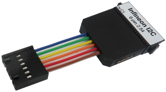
6-pin Infineon I2C (2.54mm) Debug Adapter
This debug adapter is used to connect the BlueBox to Infineon SP37/SP40 based target featuring a 6-pin 2.54mm pitch target debug connector with Infineon I2C pinout.
The debug adapter connects to the 25 cm 40-pin ribbon cable coming from the BlueBox and to the target debug connector on the other side.
The following pinout is valid on the target side:
Pin |
Signal |
Signal Description |
Signal Direction |
|---|---|---|---|
1 |
Vref |
Reference Voltage |
|
2 |
PP0 |
SCL (I2C clock line) |
I/O |
3 |
PP1 |
SDA (I2C data line) |
I/O |
4 |
GND |
Ground |
|
5 |
PP2 |
(optional) |
I/O |
6 |
PP3 |
(optional) |
I/O |
6-pin 2.54mm Infineon I2C pinout
Signal Direction is described from the BlueBox perspective.
|
When initially connecting the BlueBox to a target, ensure the debug adapter pinout matches the Target connector to avoid potential hardware failure. |
6-pin 2.54mm Infineon I2C Debug Adapter features resettable fuses on pins 1, 2, 3, 4, 5 and 6. These fuses protect debug signals against overcurrent and cycle back to a conductive state after the excessive current fades away.
Emulation Notes
The MCU can run in normal, debug or programming mode. Mode is always selected after power-on and cannot be changed later. Because of this the Vref (pin 1 on the debug connector) is a power supply output from the emulator and the target power supply (battery) must be removed while debugging. Before the debug download takes place, power off/on sequence is generated by the emulator and programming mode selected. During the debug download, first user flash is erased, then the application code programmed into the flash and at the end the complete flash is read back. This last step is required since the code memory can be no longer read once the MCU is in the debug mode. Beside of the user flash, the SP41 has also the Firmware ROM which cannot be read by the debugger.
After the debug download, the MCU is reset again since it was in the programming mode during the debug download. This means a power off/on sequence is initiated again and the debug mode selected. This same sequence is also applied when debug reset command is executed from winIDEA. During the debugging (the MCU in the debug mode) two hardware execution breakpoints are available. No software breakpoints in flash are available since the user flash cannot be modified in the debug mode. Real time access is not available.
On-chip debug logic does not implement a stop command. Therefore the MCU cannot be stopped by the debugger while the application is running. The MCU will stop only if hardware execution breakpoint is hit.
Note: The 4-pin “connector” located on the side of the debug adapter is meant for future extensions of debug functionalities. Currently it provides no functionality.
The debug adapter connects to the target via a 6-pin 2.54 mm connector, LUMBERG: 2,5 MBX 06. A target should feature a matching part, e.g., WÜRTH ELEKTRONIK: 613 006 111 21.
|
Make sure this adapter fits on your target connector - check Cross Table. |
|
Refer to Hardware Setup and Configuration Tutorial for more information on how to connect the hardware. |

