Configuration
In this topic:
•J2 and J3: Clock source configuration
•J4 - J13: Trace port configuration
•P2: Power supply configuration
•P3 – P6: Emulation device pinout
•J14 and J15: GND connecting points
|
For a detailed visual presentation of the hardware setup and configuration, refer to: |
J1: Target reset configuration
Jumper J1 connects the Emulation Adapter reset line and the user target board reset line and is populated by default. EA also features a Reset push button (SW1).
If having problems establishing the initial debug session with the Emulation Adapter, remove J1 and try again.
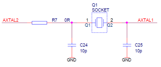
J2 and J3: Clock source configuration

Jumpers J2 and J3 select the clock source for the emulation device. The Emulation Adapter is delivered with J2 and J3 set in the default position 1-2, closer to Pin 1 marking.
Position 1-2 (default) selects the crystal circuit oscillator on the target board. To select the crystal circuit oscillator on the Emulation Adapter (Q1 socket), set:
1. Set both Jumpers J2 and J3 away from Pin 1 marking.
2. Insert the crystal circuit delivered with the Emulation Adapter into the Q1 socket.
|
The Emulation Adapter may not operate when the target board’s crystal circuit is used as the clock source. A typical design guideline is that the crystal should be as close as possible to the SoC. The target crystal might not oscillate in conjunction with the Emulation Adapter since the clock lines between the target crystal and the emulation device on the Emulation Adapter become too long, thus affecting the impedance of the crystal circuit. |

|
Separately packed 16 MHz crystal can be used as a 16 MHz external clock (XOSC) source to the emulation device. If a different clock frequency is required, insert an adequate crystal into the Q1 socket and replace C24 (default 10 pF populated) and C25 (default 10 pF populated) accordingly. Crystal socket Q1 is by default not populated (NP). |
Crystal socket Q1 below:
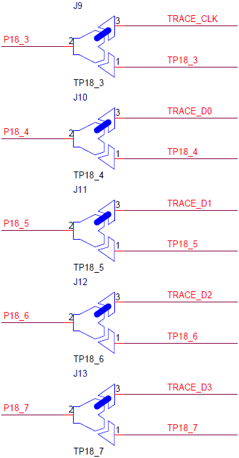
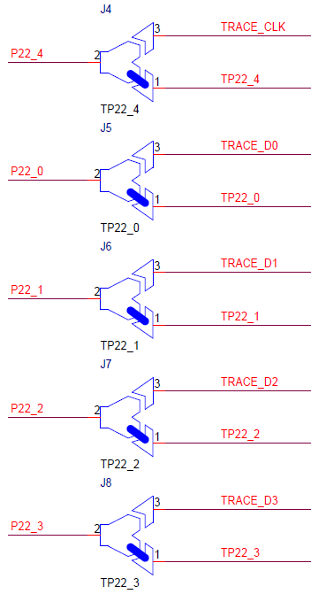
J4 - J13: Trace port configuration
Soldered jumpers are by default placed to connect ARM CoreSight 20 connector trace signals to port P18 (J9 – J13). If P18 on user target board is used for any other purpose than trace, Emulation Adapter allows changing the trace source to port P22 (J4 – J8) with relocation of the jumpers.
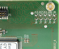
Soldered jumpers J4-J13 on EA on the image below:
|
|
Default position on P18 |
Optional position on P22 |
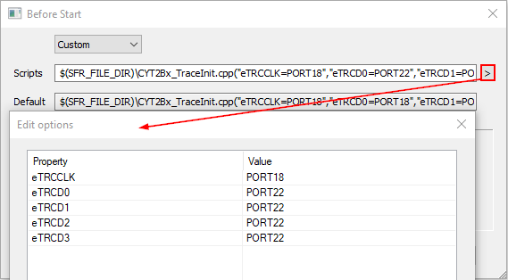
winIDEA configuration
By default, P18 port pins (P18_3 – P18_7) or P22 port pins (P22_0 – P22_4) are set as GPIO pins. To configure these pins as trace pins in winIDEA, open Hardware | CPU Options | Analyzer and add a script CYT2Bx_TraceInit.cpp in the SoC Initialization section. Allocate via the Parameters options and depending on the user target board configuration:
•TRACE CLOCK Port to PORT 18 (or PORT 22)
•TRACE DATAn PORT to PORT 18 (or PORT 22)
P2: Power supply configuration
Emulation Adapter Power supply is configured via the unshrouded 26-pin 2.54 mm header (P2).
Signal direction |
Signal |
Pin |
Pin |
Signal |
Signal direction |
|---|---|---|---|---|---|
Target board |
VDDA |
1 |
2 |
CVDDA |
Emulation device |
Target board |
VREFH |
3 |
4 |
CVREFH |
Emulation device |
Not Connected |
NC |
5 |
6 |
NC |
Not Connected |
Target board |
VDDIO_1 |
7 |
8 |
CVDDIO_1 |
Emulation device |
Target board |
VDDIO_2 |
9 |
10 |
CVDDIO_2 |
Emulation device |
Target board |
VDDD |
11 |
12 |
CVDDD |
Emulation device |
Not Connected |
NC |
13 |
14 |
NC |
Not Connected |
Not Connected |
NC |
15 |
16 |
NC |
Not Connected |
Not Connected |
NC |
17 |
18 |
NC |
Not Connected |
Not Connected |
NC |
19 |
20 |
NC |
Not Connected |
Ground |
GND |
21 |
22 |
GND |
Ground |
Ground |
GND |
23 |
24 |
GND |
Ground |
Ground |
GND |
25 |
26 |
KEY |
|
P2 Signal description
Signal Direction is described from the BlueBox perspective.
By default, all jumpers are set to connect your target power supply to the microcontroller residing on the Emulation Adapter. Only pins 1-2, 3-4, 7-8, 9-10 and 11-12 must be bridged but for the convenience and ease of use all jumpers are set, except for pins 5-6 and 25-26.
Pin 26 is the polarizer key preventing incorrect connection of the IEA-PS Power converter, when being plugged in.
If a different power source is used (e.g. a Standalone operation), remove all jumpers and apply 3V3 or 5V to:
•CVDDA (pin 2)
•CVREFH (pin 4, apply the same voltage as on VDDA)
•CVDDIO_1 (pin 8)
•CVDDIO_2 (pin 10)
•CVDDD (pin 12)
Enclosed Power supply package (Power converter and Power adapter) simply plugs into the P2 header row, providing the necessary power supply for Emulation Adapter operation.
LED D1 indicates, if power is supplied to the Emulation Adapter. Refer to the microcontroller documentation for more details about power voltage designations.
P3 – P6: Emulation device pinout
P3, P4, P5, P6 pinouts match the pinout of the emulation device (176QFP). Refer to the microcontroller documentation for pin assignment.
J14 and J15: GND connecting points
J14 and J15 provide grounding points on the Emulation Adapter.