Configuration
In this topic:
•J2 and J3: Clock source configuration
•J4 & J5: GND connecting points
•Startup and Power Supply Mode
•P2: Power supply configuration
|
For a detailed visual presentation of the hardware setup and configuration, refer to: |
J1: Target reset configuration
Jumper J1 connects the TC234LF reset line (PORST) and the target reset line. By default J1 is populated.
When having problems establishing the initial debug session with the emulation adapter, try to remove J1 and see if it makes any difference.
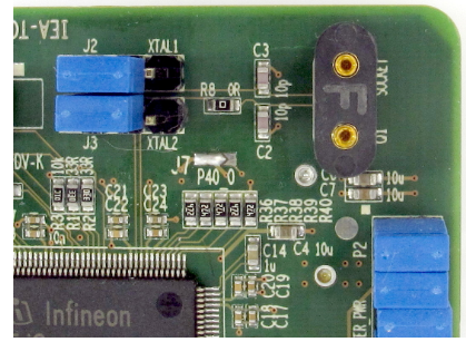
J2 and J3: Clock source configuration
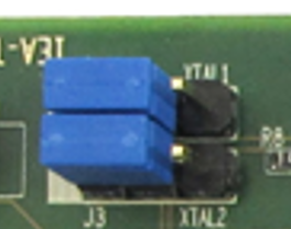
Jumpers J2 and J3 select the clock source for the emulation device. The Emulation Adapter is delivered with J2 and J3 set in the default position 1-2, closer to Pin 1 marking.
Position 1-2 (default) selects the crystal circuit oscillator on the target board. To select the crystal circuit oscillator on the Emulation Adapter (Q1 socket), set:
1. Set both Jumpers J2 and J3 away from Pin 1 marking.
2. Insert the crystal circuit delivered with the Emulation Adapter into the Q1 socket.
|
The Emulation Adapter may not operate when the target board’s crystal circuit is used as the clock source. A typical design guideline is that the crystal should be as close as possible to the SoC. The target crystal might not oscillate in conjunction with the Emulation Adapter since the clock lines between the target crystal and the emulation device on the Emulation Adapter become too long, thus affecting the impedance of the crystal circuit. |

|
Separately packed 20 MHz crystal can be used as a 20 MHz external clock (XOSC) source to the emulation device. If a different clock frequency is required, insert appropriate crystal into the Q1 socket and replace C1 (default 10 pF populated) and C2 (default 10 pF populated) accordingly. Crystal socket Q1 is by default not populated (NP). |
The crystal circuit is located in the corner of the emulation adapter.
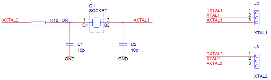
Note that C1 and C2 values are valid for 20MHz crystal only. If different crystal is used, the default 10 pF capacitors must be replaced with a proper value.
J4 & J5: GND connecting points
The original microcontroller in the QFP100 package provides GND connection through the exposed pad. The emulation adapter, replacing the original microcontroller doesn’t provide support for the exposed pad and for this reason the GND connection must be established separately. Use J4 or J5 connection pin to established good GND connection between the emulation adapter and the target. The connection should be quality and short as possible. Refer to the Emulation Notes chapter for potential problems with this grounding connection.
J9 & J10
If the emulation adapter is attached to the target, jumpers J9 and J10 must not be populated since the target takes care of all the microcontroller pin connections already.
When the emulation adapter is to be used in a so called standalone operation without connecting it to the target, and the microcontroller analog/digital converter is used, the two jumpers should be set. Jumper J9 connects VAGND to VSSM and jumper J10 connects VSSM to the emulation adapter GND potential.
•VAGND (pin 41) – Negative Analog Reference Voltage 0
•VDDM (pin 44) – ADC Power Supply
•VSSM (pin 43) Analog Ground for VDDM
Emulation Notes
|
This emulation adapter is custom designed for use with specific target and is not meant for general use! |
Original microcontroller connects the GND potential to the target PCB through the exposed pad located in the center of the microcontroller on the bottom side of the package”.
The emulation adapter connects to the target PCB via Solder part which doesn’t provide the exposed pad. That means ground signal remains unconnected. No solder part supporting this QFP100 (0.4 mm pitch) package featuring exposed pad exists in the market (status 2017/Q4). For this reason, emulation adapter provides a dedicated GND connection through a short wire, which has to be connected between the emulation adapter and the target. Note that such setup could exhibit problems since the ground potential is not routed close to the microcontroller pins and the GND path is considerably prolonged comparing to the original microcontroller with the GND connected through the exposed pad.
4k7 ohm pull-up is present on the port P14.2 and 4k7 ohm pull-downs are present on the following ports:
•P00.1-P00.9, P00.12, •P10.1-P10.3, •P14.5, P14.7, P14.8 •P15.4. P15.6-P15.8, •P20.0, P20.3, P20.6, P20.7, |
•P21.5, •P22.0-P22.4, •P33.0-P33.4, P33.11, P33.12 •P34.0-P34.3 |
These ports exist on the 144-pin device, which is populated on the emulation adapter, while the 100-pin target device being emulated by the emulation adapter doesn’t have these ports. These resistors predefine value of these ports when their input registers are read by the application. This makes sense only when the same application is supposed to run on 100-pin and 144-pin microcontroller. If the application is written for 100-pin device only, it shouldn’t read these ports since they don’t exist.
At the moment 144-pin TC234LF AB step is populated on the emulation adapter. For the 100-pin TC233LP target device, newer AC step exists already, fixing known issues from the AB step including CAN FD related issues. Refer to Infineon errata documents for more details on known issues and fixes for specific step. Infineon has no plans to do an AC step of the 144-pin TC234LF emulation device (status: 2017/Q1). Consequentially, the application running on the target based on a real 100-pin TC233LP device step AC or newer can behave differently comparing to the application running on the TC234LF emulation adapter.
Startup and Power Supply Mode
The target device TC234 being emulated with this emulation adapter, can have the external nominal system supply either 3.3V or 5V. Both are supported by the emulation adapter. The power supply scheme of the TC234LF at startup is based on the latched status of HWCFG[0:2] pins before PORST release. With the emulation adapter, HWCFG[0:2, 6] pins are left unconnected (floating) while the TC234LF PORST signal is low. This ensures embedded voltage regulators EVR33 and EVR13 are active by default. As soon as the PORST line is released from the low state, the HWCFG[0:2, 6] pins get connected to the target via the emulation adapter logic.
P2: Power supply configuration
Emulation Adapter Power supply is configured via the unshrouded 26-pin 2.54 mm header (P2).
Signal Direction |
Signal |
Pin |
Pin |
Signal |
Signal Direction |
|---|---|---|---|---|---|
target |
VDDP3 |
1 |
2 |
CVDDP3/3v3 |
CPU |
target |
VDDM |
3 |
4 |
CVDDM |
CPU |
target |
VAREF |
5 |
6 |
CVAREF |
CPU |
|
NC |
7 |
8 |
NC |
|
|
NC |
9 |
10 |
NC |
|
|
NC |
11 |
12 |
NC |
|
|
NC |
13 |
14 |
NC |
|
|
NC |
15 |
16 |
NC |
|
|
NC |
17 |
18 |
NC |
|
|
NC |
19 |
20 |
NC |
|
|
GND |
21 |
22 |
GND |
|
|
GND |
23 |
24 |
GND |
|
|
GND |
25 |
26 |
KEY |
|
P2 Signal description
Refer to the microcontroller user’s manual for more details which power supply designation in the above table belongs to which power supply.
By default all jumpers are set and connect target power supply coming from the target to the microcontroller residing on the emulation adapter. In principle, pins 3-4, 5-6, 7-8, must be bridged only but for the convenience and ease of use, all jumpers are set except for pins 25-26. Pin 26 is the polarizer key preventing incorrect connection of the IEA-PS power supply, when connected.