Configuration
In this topic:
•J2 and J3: Clock source configuration
•J5 & J6: GND connecting points
•Startup and Power Supply Mode
•P2: Power supply configuration
|
For a detailed visual presentation of the hardware setup and configuration, refer to: |
J1: Target reset configuration
Jumper J1 connects the TC265DE reset line (PORST) and the target reset line. By default J1 is populated.
When having problems establishing the initial debug session with the emulation adapter, try to remove J1 and see if it makes any difference.
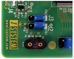
J2 and J3: Clock source configuration
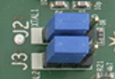
Jumpers J2 and J3 select the clock source for the emulation device. The Emulation Adapter is delivered with J2 and J3 set in the default position 1-2, closer to Pin 1 marking.
Position 1-2 (default) selects the crystal circuit oscillator on the target board. To select the crystal circuit oscillator on the Emulation Adapter (Q1 socket), set:
1. Set both Jumpers J2 and J3 away from Pin 1 marking.
2. Insert the crystal circuit delivered with the Emulation Adapter into the Q1 socket.
|
The Emulation Adapter may not operate when the target board’s crystal circuit is used as the clock source. A typical design guideline is that the crystal should be as close as possible to the SoC. The target crystal might not oscillate in conjunction with the Emulation Adapter since the clock lines between the target crystal and the emulation device on the Emulation Adapter become too long, thus affecting the impedance of the crystal circuit. |

|
Separately packed 20 MHz crystal can be used as a 20 MHz external clock (XOSC) source to the emulation device. If a different clock frequency is required, insert appropriate crystal into the Q1 socket and replace C1 (default 10 pF populated) and C2 (default 10 pF populated) accordingly. Crystal socket Q1 is by default not populated (NP). |
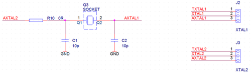
Note that C1 and C2 values are valid for 20MHz crystal only. If different crystal is used, the default 10 pF capacitors must be replaced with a proper value.
J5 & J6: GND connecting points
J5 and J6 provide grounding points on the Emulation Adapter.
In case a good ground connection is required, connection points bridge J5 and pin J6 provide easy access to the emulation adapter GND potential.
Startup and Power Supply Mode
The target device TC265 being emulated with this emulation adapter, can have the external nominal system supply either 3.3V or 5V. Both are supported by the emulation adapter. The power supply scheme of the TC265DE at startup is based on the latched status of HWCFG[0:2] pins before PORST release. With the emulation adapter, HWCFG[0:2, 6] pins are left unconnected (floating) while the TC265DE PORST signal is low. This ensures embedded voltage regulators EVR33 and EVR13 are active by default. As soon as the PORST line is released from the low state, the HWCFG[0:2, 6] pins get connected to the target via the emulation adapter logic.
P2: Power supply configuration
Emulation Adapter Power supply is configured via the unshrouded 26-pin 2.54 mm header (P2).
Signal Direction |
Signal |
Pin |
Pin |
Signal |
Signal Direction |
|---|---|---|---|---|---|
Target board |
NC |
1 |
2 |
NC |
Emulation device |
Target board |
VEXT |
3 |
4 |
CVEXT |
Emulation device |
Target board |
VDDM |
5 |
6 |
CVDDM |
Emulation device |
Target board |
VFLEX |
7 |
8 |
CVFLEX |
Emulation device |
|
NC |
9 |
10 |
NC |
|
|
NC |
11 |
12 |
NC |
|
|
NC |
13 |
14 |
NC |
|
|
NC |
15 |
16 |
NC |
|
|
NC |
17 |
18 |
NC |
|
|
NC |
19 |
20 |
NC |
|
|
GND |
21 |
22 |
GND |
|
|
GND |
23 |
24 |
GND |
|
|
GND |
25 |
26 |
KEY |
|
P2 Signal description
NC – Not Connected
Refer to the microcontroller user’s manual for more details which power supply designation in the above table belongs to which power supply.
By default all jumpers are set and connect target power supply coming from the target to the microcontroller residing on the emulation adapter. In principle, pins 3-4, 5-6, 7-8, must be bridged only but for the convenience and ease of use all jumpers are set, except for pins 25-26. Pin 26 is the polarizer key preventing incorrect connection of the IEA-PS power supply, when connected.