SPI
This chapter describes how configure and provide network description for the Network analyzer ADIO - SPI.
Using digital inputs, optional SPI protocol analyzer is available for easy monitoring of two SPI interfaces (SPI1, SPI2) within the embedded system either alone or in conjunction with the program execution.
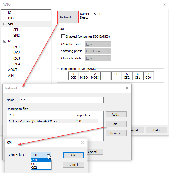
Network
Name - Give the network a meaningful name.
Add - Add SPI description files (*.spi). Find TASKING SPI protocol description format here...
Edit - Open SPI dialog to select chip (CS0, CS1, CS2).
SPI - Enabled - SPI modules are by default disabled because they consume DIO BANKS (Digital I/O connectors).
CS Active state - Low, High - Active state is configurable.
Sampling phase - First Edge, Second Edge - Select the rising or falling edge of the clock to sample and/or shift the data.
Clock idle state - Low, High - Select the idle state.
Pin mapping on DIO BANK0/BANK2 - Description of pin connections for SPI protocol. Make sure that pin mapping is set correctly. Refer to SPI protocol description format for more information.
|
When SP1 is enabled it consumes DIO BANK0. When SP2 is enabled it consumes DIO BANK2. |