JTAG page dialog reference
Open Hardware > SoC Options > JTAG.
This page is hidden when Debug Protocol > Channel other than JTAG is selected in the SoC page.
|
This page is hidden when Debug Protocol > Channel other than JTAG is selected in the SoC page. |

Scan speed
Scan speed depends on the SoC clock and Target board Hardware design guidelines.
|
JTAG Scan speed 1000 kHz (default) should work in most cases. However, if the debug connection cannot be established with the Target or the debug session behaves unreliably, try frequencies in the range from 1 to 5 MHz. A value in kHz can be manually typed in. If it still doesn’t work, go further below 1MHz until you find a working setting. |

Number of idle TCKs
Define number of trailing TCK cycles after JTAG scan returns to Test-Logic-Idle JTAG state. Can be used to increase communication robustness at higher JTAG speeds.
Use Scan speed during Initialization
This option is useful on systems which start very slow. Slower scan speed can be used for first initialization sequence (see Initialization Sequence details), during which the SoC clock is raised (PLL engaged) and then higher scan speeds can be used for program and later while debugging.
Do not use TRST line
Enable this when assertion of JTAG TRST line is not desired. TAP will be reset only by clocking through Test-Logic-Reset JTAG state.
JTAG chain
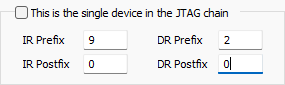
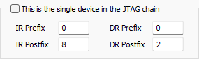
Enable option This is the single device in the JTAG chain when only target SoC is connected to debug connector. Multiple TAPs inside target SoC are handled by winIDEA accordingly to the SoC selection. The scan frequency of the Test Access Port (TAP) is typically synchronized with the target SoC's system clock and is generally a few times slower.
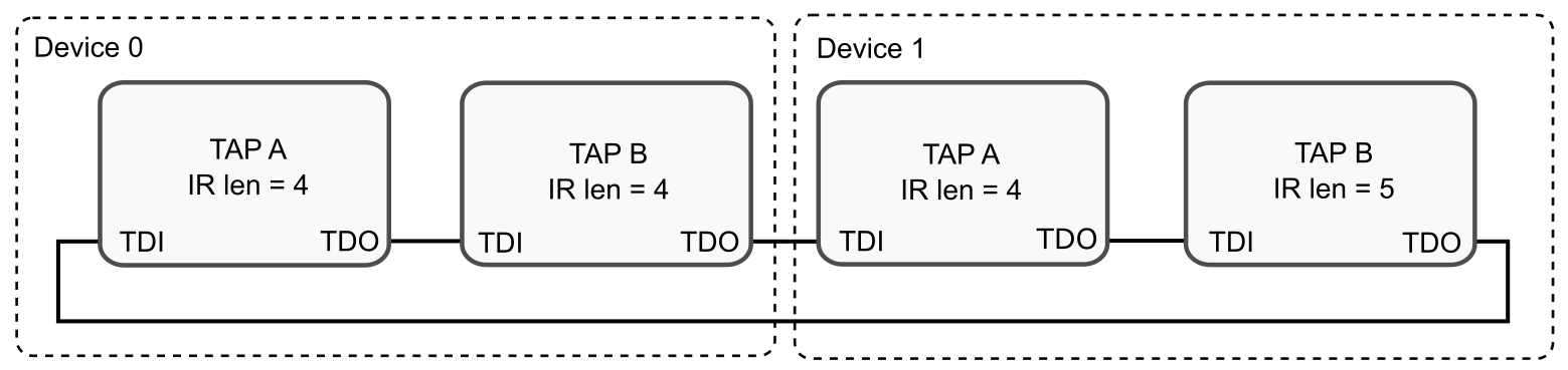
When the JTAG chain contains multiple TAPs, the configuration of the Instruction Register (IR) and Data Register (DR) prefixes and postfixes is crucial:
•IR Prefix to the sum of IR lengths of all following* TAPs
•IR Postfix to the sum of IR lengths of all preceding* TAPs
•DR Prefix to the number of following* TAPs
•DR Postfix to the number of preceding* TAPs
* In a topology sense in direction from Test Data Input (TDI) to Test Data Output (TDO). Pre/post terminology was chosen based on when filling bits need be shifted into TDI.
Example of the JTAG chain
|
Device 0 |
Device 1 |
|---|---|---|
IR Prefix |
4 + 5 = 9 |
0 |
IR Postfix |
0 |
4 + 4 = 8 |
DR Prefix |
2 |
0 |
DR Postfix |
0 |
2 |
winIDEA settings |
|
|