Configuration
In this topic:
•J2 and J3 : Clock source configuration
•J4 and J5: GND connection points
•P2: Power supply configuration
|
For a detailed visual presentation of the hardware setup and configuration, refer to: |
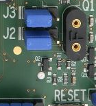
J1: Target reset configuration
Jumper J1 connects the Emulation Adapter reset line and the user target board reset line and is populated by default.
Emulation Adapter features a Reset push button (SW1).
If having problems establishing the initial debug session with the Emulation Adapter, remove J1 and try again.
J2 and J3 : Clock source configuration
Jumpers J2 and J3 select the clock source for the emulation device. The Emulation Adapter is delivered with J2 and J3 set in the default position 1-2, closer to Pin 1 marking.
Position 1-2 (default) selects the crystal circuit oscillator on the target board. To select the crystal circuit oscillator on the Emulation Adapter (Q1 socket), set:
1. Set both Jumpers J2 and J3 away from Pin 1 marking.
2. Insert the crystal circuit delivered with the Emulation Adapter into the Q1 socket.
|
The Emulation Adapter may not operate when the target board’s crystal circuit is used as the clock source. A typical design guideline is that the crystal should be as close as possible to the SoC. The target crystal might not oscillate in conjunction with the Emulation Adapter since the clock lines between the target crystal and the emulation device on the Emulation Adapter become too long, thus affecting the impedance of the crystal circuit. |

|
Separately packed 20 MHz crystal can be used as a 20 MHz external clock (XOSC) source to the emulation device. If a different clock frequency is required, insert appropriate crystal into the Q1 socket and replace C7 (default 10 pF populated) and C8 (default 10 pF populated) accordingly. Crystal socket Q1 is by default not populated (NP). |
Crystal socket Q1 schematics below:

J4 and J5: GND connection points
In case a good ground connection is required, connection points bridge J4 and pin J5 provide easy access to the Emulation Adapter's GND potential.

J6 and J7: VFLEX and VAREF
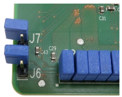
VFLEX - If the target’s VFLEX pin isn’t exposed, bridge the jumper J6 to connect VEXT from the target to power VFLEX.
|
Setting the jumper when emulating the BGA device may prevent establishing a debug connection or, in the worst case, can damage the Target board. |
VAREF - If the target’s VAREF2 pin isn’t exposed, bridge the jumper J7 to connect VAREF1 from the target to power VAREF2
|
Setting the jumper if VAREF2 is present on the device may prevent establishing a debug connection or, in the worst case, can damage the Target board. |
P2: Power supply configuration
Power supply of the Emulation Adapter is configured via the unshrouded 26-pin 2.54 mm header (P2).
Signal direction |
Signal |
Pin |
Pin |
Signal |
Signal direction |
|---|---|---|---|---|---|
Target board |
TVEXT |
1 |
2 |
VEXT |
Emulation device |
Target board |
TVDDM |
3 |
4 |
VDDM |
Emulation device |
Target board |
TVAREF1 |
5 |
6 |
VAREF1 |
Emulation device |
Target board |
TVAREF2 |
7 |
8 |
VAREF2 |
Emulation device |
Target board |
TVEVRSB |
9 |
10 |
VEVRSB |
Emulation device |
Target board |
TVFLEX |
11 |
12 |
VFLEX |
Emulation device |
Not connected |
NC |
13 |
14 |
NC |
Not connected |
Not connected |
NC |
15 |
16 |
NC |
Not connected |
Not connected |
NC |
17 |
18 |
NC |
Not connected |
Not connected |
NC |
19 |
20 |
NC |
Not connected |
Ground |
GND |
21 |
22 |
GND |
Ground |
Ground |
GND |
23 |
24 |
GND |
Ground |
Ground |
GND |
25 |
26 |
KEY |
|
P2 Signal description
By default, all jumpers are set to connect user target power supply to the microcontroller residing on the Emulation Adapter. Only pins 1-2, 3-4, 5-6, 7-8, 9-10 and 11-12 must be bridged, but for the convenience and ease of use, all jumpers are set, except for pins 25-26.
Pin 26 is the polarizer key preventing incorrect connection of the IEA-PS Power converter, when being plugged in.
If a different power source is used (e.g., a Standalone operation), remove all jumpers and apply 3V3 or 5V to:
•VEXT (pin 2), •VDDM (pin 4), •VAREF1 (pin 6), |
•VAREF2 (pin 8), •VEVRSB (pin 10), •VFLEX (pin 12). |
Enclosed Power supply package (Power converter and Power adapter) simply plugs into the P2 header row, providing the necessary power supply for Emulation Adapter operation. LED1 indicates if power is supplied to the Emulation Adapter.
Refer to the microcontroller documentation for more details about power voltage designations.
Connectors
|
Be aware that debug and trace signals from the Emulation Adapter superset device are not connected to the target board. They are exposed only to the connectors on the Emulation adapter. |
P1: DAP
P1 connector exposes DAP debug interface.
Signal Direction |
Signal Description |
Signal |
Pin |
Pin |
Signal |
Signal Description |
Signal Direction |
|---|---|---|---|---|---|---|---|
I |
Reference Voltage |
Vref |
1 |
2 |
DAP1 |
DAP Data pin |
I/O |
|
Ground |
GND |
3 |
4 |
DAP0 |
DAP clock |
O |
|
Ground |
GND |
5 |
6 |
DAP2 |
Optional 2d DAP Data pin |
I/O |
|
Not Connected |
NC |
7 |
8 |
DAPEN |
DAP Enable |
O |
|
Ground |
GND |
9 |
10 |
nRESET |
Reset |
I/O |
10-pin Infineon DAP pinout
Signal Direction is described from the BlueBox perspective.
BlueBox supporting Infineon DAP debug and trace interface connects to the P1 connector.
P8: DAPE
P8 connector exposes DAPE debug interface.
Signal Direction |
Signal Description |
Signal |
Pin |
Pin |
Signal |
Signal Description |
Signal Direction |
|---|---|---|---|---|---|---|---|
I |
Reference Voltage |
Vref |
1 |
2 |
DAPE1 |
DAP Data |
I/O |
|
Ground |
GND |
3 |
4 |
DAPE0 |
DAP Clock |
O |
|
Ground |
GND |
5 |
6 |
DAPE2 |
Optional 2nd Data Pin |
I/O |
|
Not Connected |
NC |
7 |
8 |
DAPEN/DAP3 |
Optional 3rd Data Pin |
I/O |
|
Ground |
GND |
9 |
10 |
NC |
Not Connected |
|
10-pin DAPE pinout
Signal Direction is described from the BlueBox perspective.
BlueBox supporting Infineon DAPE debug and trace interface connects to the P8 connector.
P7: AGBT
P7 connector exposes AGBT interface.
Signal Direction |
Signal Description |
Signal |
Pin |
Pin |
Signal |
Signal Description |
Signal Direction |
|---|---|---|---|---|---|---|---|
I |
AGBT TX0_P |
TX0_P |
1 |
2 |
Vref |
Reference Voltage |
I |
I |
AGBT TX0_N |
TX0_N |
3 |
4 |
DAP0 |
DAP clock |
O |
|
Ground |
GND |
5 |
6 |
DAP1 |
DAP Data pin |
I/O |
|
Not Connected |
NC |
7 |
8 |
NC |
Not Connected |
|
|
Not Connected |
NC |
9 |
10 |
DAP2 |
Optional 2nd Data pin |
I/O |
|
Ground |
GND |
11 |
12 |
nTRST/DAPEN |
JTAG/Output |
O |
|
Not Connected |
NC |
13 |
14 |
CLK+ |
AGBT Clock |
O |
|
Not Connected |
NC |
15 |
16 |
CLK- |
AGBT Clock |
O |
|
Ground |
GND |
17 |
18 |
TGO* |
AGBT Trigger out |
I |
|
Not Connected |
NC |
19 |
20 |
AGBT ERR |
AGBT Error |
|
|
Not Connected |
NC |
21 |
22 |
RESET |
Reset |
I/O |
22-pin AGBT pinout (Revision C1)
Signal Direction is described from the BlueBox perspective.
Blue color marks the trace signals.
* Pin 18: TGO (AGBT Trigger out) is connected to the pin TP32.6. Before Revision C1 pin 18 was NC (Not Connected).
BlueBox solution supporting AGBT (Aurora GigaBit Trace) interface connects to the P7 connector.
Power supply
Use the enclosed IEA-PS Emulation Adapter Power converter and adapter. A Power supply package, which is delivered with the Emulation Adapter, is required when:
•The Emulation Adapter is used as a standalone device.
•The target board doesn’t provide an accurate supply voltage.
•The target board doesn’t provide sufficient current for the Emulation Adapter operation.
The Power converter can supply either 3.3 V or 5 V. The array of jumpers J0–J9 selects 3.3 V or 5 V voltage on the P3 connector, which connects to the Emulation Adapter.
Signal |
Pin |
Pin |
Signal |
|---|---|---|---|
NC |
1 |
2 |
J0 |
NC |
3 |
4 |
J1 |
NC |
5 |
6 |
J2 |
NC |
7 |
8 |
J3 |
NC |
9 |
10 |
J4 |
NC |
11 |
12 |
J5 |
NC |
13 |
14 |
J6 |
NC |
15 |
16 |
J7 |
NC |
17 |
18 |
J8 |
NC |
19 |
20 |
J9 |
GND |
21 |
22 |
GND |
GND |
23 |
24 |
GND |
GND |
25 |
26 |
KEY |
P3 connector and J0–J9 jumper correlation table
For example, when J2 is in the 3V3 position, it supplies 3.3 V to pin 6 of the P3 connector. When J2 is in the 5V position, it supplies 5 V to pin 6 of the P3 connector pin.
|
Be careful not to supply 5 V to the microcontroller power supply pin, which has declared a maximum voltage 3.3 V! Refer to the microcontroller documentation for detailed information on power supply. |
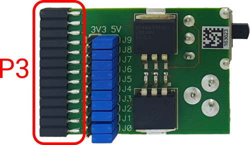
P3 connector on the Power Supply board
External power supply requirements:
Min Voltage |
Max Voltage |
Min Power |
|
|---|---|---|---|
8 V |
12 V |
18 W |
Clock source
If the target’s crystal circuit microcontroller oscillator (if available) is not an adequate clock source, insert appropriate crystal into the Q1 socket, replace the default 10pF C7 and C8 capacitors when necessary and place jumpers J2 and J3 in 2-3 position.