ADIO Use cases overview
In this topic:
•AOUT, AIN, SPI and Pattern Generator
For the how-to guide refer to ADIO Use cases Configuration.
General use cases
Following use cases depict connection possibilites of digital/analog input/output connectors and embedded target, winIDEA plugin HIL Monitor provides the monitoring and manipulation capability of the input/output signals. All monitored signals can be also traced with the winIDEA Analyzer.
Observing digital inputs
1.First connect ground potential (GND) of the Digital I/O connector with the monitored embedded system ground (GND) using provided clip wires. Note that all eight GND signals of each Digital I/O connector are internally connected.
2.Use clip wires to connect signals from the embedded system to the pins of Digital I/O connector D0 (or D1 or D2 or D3).
3.Configure used Digital I/O connector (D0 or D1 or D2 or D3) for input operation and its input voltage range in winIDEA. Note that all eight signals of the selected Digital I/O connector are set as inputs.
Configured input (or output) operation for the individual Digital I/O connector applies to all 8 available digital signals on the connector. Mixing input and output signals within one Digital I/O connector is not supported.
Observing analog inputs
Use standard oscilloscope probes to connect analog inputs AIN0 respectively AIN1 to the embedded system.
Output analog signal
1.First connect ground potential (GND) of the AOUT0, AOUT1 connector with the embedded system ground (GND) using provided clip wires. All five GND signals of the AOUT0, AOUT1 connector are internally connected.
2.Use clip wires to connect AOUT0 respectively AOUT1 pin to the Embedded system.
3.Voltage output range is configured in winIDEA.
Output digital signals
1.First connect ground potential (GND) of the Digital I/O connector with the embedded system ground (GND) using provided clip wires. All eight GND signals of each Digital I/O connector are internally connected.
2.Use clip wires to connect signals from the embedded system to the pins of Digital I/O connector D0 (or D1 or D2 or D3).
3.Configure used Digital I/O connector (D0 or D1 or D2 or D3) for output operation and its output voltage range in winIDEA. Note that all eight signals of the selected Digital I/O connector are set as inputs.
Configured output (or input) operation for the individual Digital I/O connector applies to all 8 available digital signals on the connector. Mixing input and output signals within one Digital I/O connector is not supported.
Close-up SPI recording
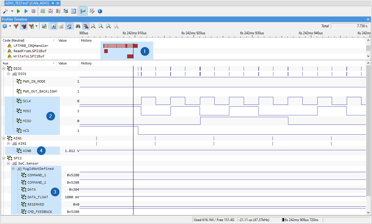
The target executes the interrupt routine, from which it calls the function WriteToLSPI1Buf (1), which writes the data to be sent on the MOSI line. So the SPI master (the target’s SPI peripheral) lowers the chip select line, activates the SCLK and starts sending the message (2). As per configuration of the SPI Slave (the ADC converter), ADC will respond on the MISO line.
The messages can be decoded even in this state, that is from the bitstream on the recorded digital inputs, but this is rather tiresome and time consuming. This is where the SPI protocol analyzer steps in. Using the SPI description file mentioned previously, you are able to display the enumerated values of the defined fields in the analyzed SPI message (3).
For instance, you have defined that the MOSI data will always comprise of two identical 16bit command words (COMMAND_1 and COMMAND_2), which in this case have the value 0x528B (this tells the ADC to return the result from the ADC Channel 1). The ADC returns the 12bit converted value - DATA , followed by the RESERVED 4bits, and by a 2B COMMAND_FEEDBACK which in this case also has the same value as the commands issued by the target.
For further convenience it is that the read DATA be converted and displayed as a number of mV measured by the ADC channel - noted by the DATA_FLOAT signal.
For comparison, the analog input is recorded (4), which measures the same voltage as the ADC Channel 1, and displayed in the same recording.
AOUT, AIN, SPI and Pattern Generator
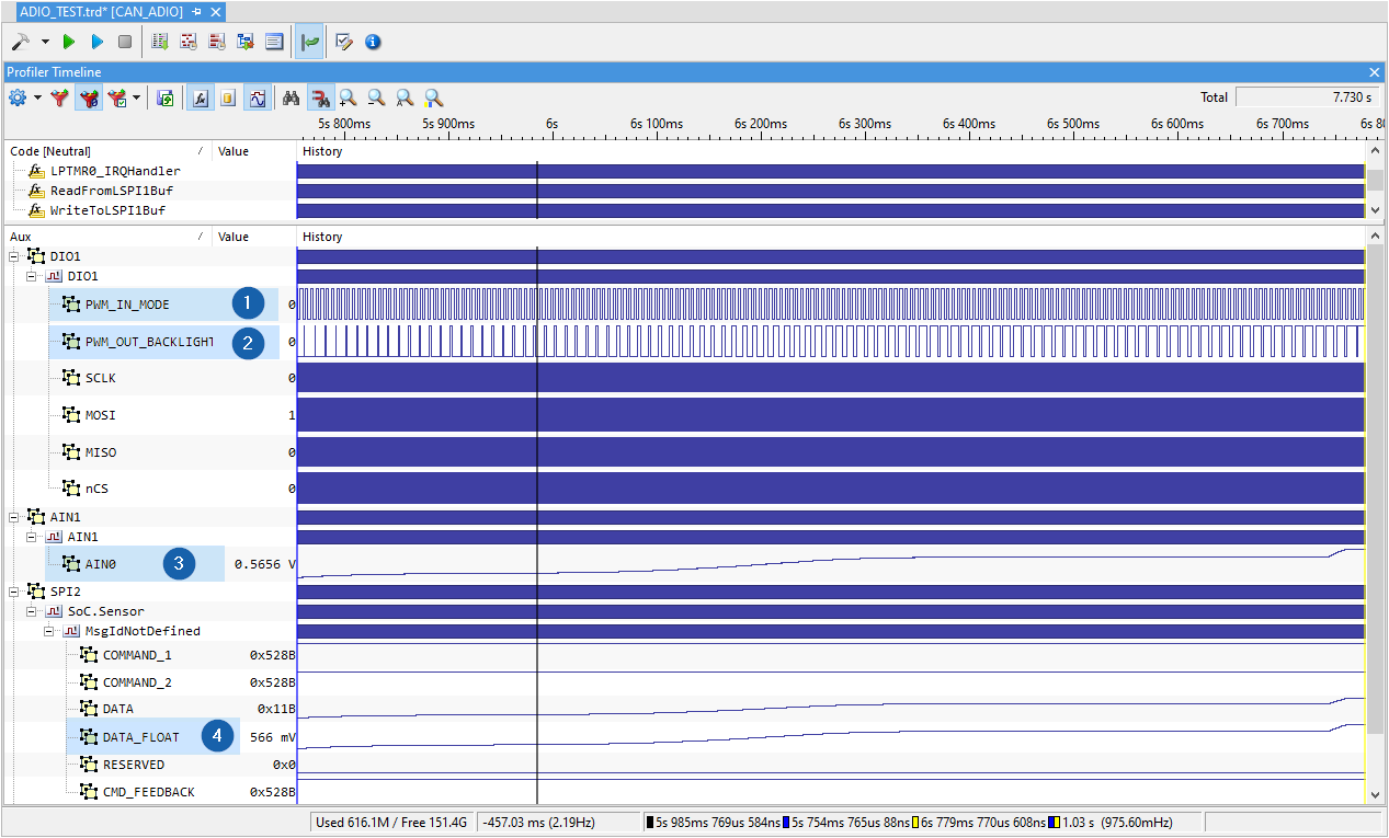
Analyzer depicts a longer recording and shows how a combination of the ADIO capabilities is used to fit the many possible uses. For instance, the Pattern Generator generates continuously a 200Hz square wave signal (1), which configures the target to work in Automatic mode - i.e. generate output (2) based on the readings from the SPI.
Then you use the Analog output voltage to gradually increase the voltage on an LED, which is directed towards an illumination sensor. The sensor has a voltage output, which is connected to both AIN0 channel (3) of the ADIO , and Channel 1 of the external ADC (4). It can clearly be seen that the output signal duty ratio increases with the rise of the LED voltage.
Alternative
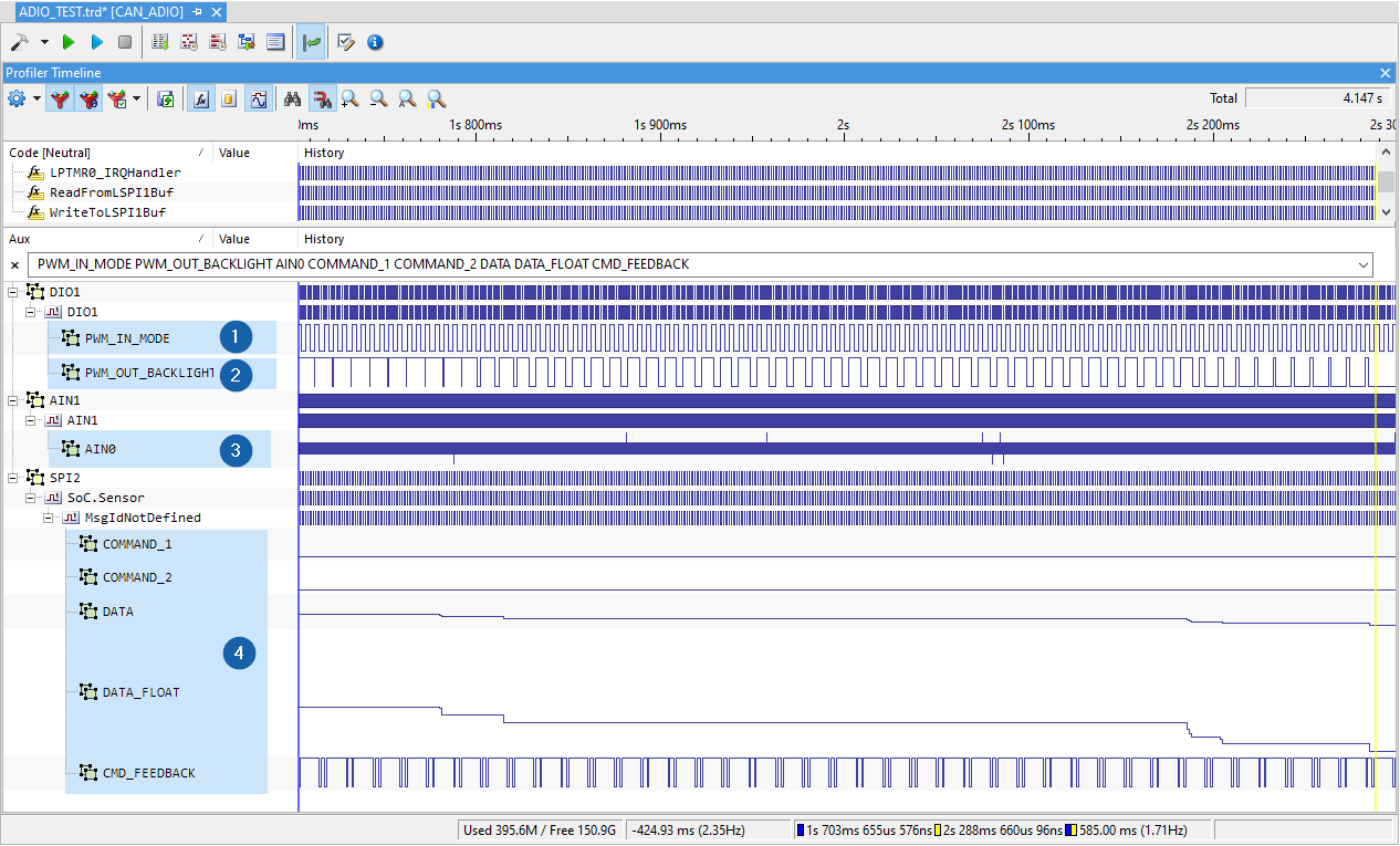
This use case is similar to the previous one (the combination of ADIO capabilities used simultaneously), but in this case external components are replaced with an AOUT channel.
AOUT[LED_VDD] controls the voltage of an LED, which illuminates the sensor, and reads the sensor output via the external ADC. In this case both the LED and the Sensor are replaced with an AOUT channel, which allows to simplify the hardware requirements without losing any of the functionality.
The target is still in the Automatic mode (1). The actual sensor output remains unchanged throughout the test (3), while the AOUT[Sensor_Vout] voltage decrease is reflected in the read data from the SPI (4). The conversion results of the ADC Channel 0 is read, which is the Sensor_Vout signal that is controlled. As the Sensor_Vout decreases, so does the pulse width of the PWM_OUT_BACKLIGHT signal (2).
Pattern Generator
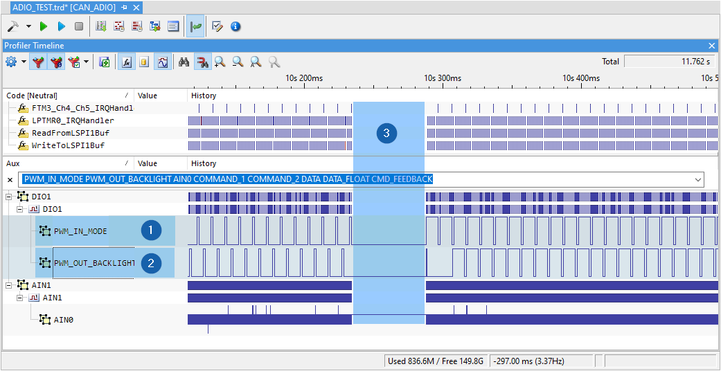
This use case shows when the target is put to the Manual mode by the ADIO. This is done by reconfiguring the Pattern generator to generate a 100Hz square wave (1.) in which case the target output will follow the input signal (2.). Note that the current implementation of the ADIO requires some time for re-configuration of the Pattern Generator, which can be noticed as a gap in the Analyzer recording (3). In this example, the Pattern Generator was originally configured to produce a 15% duty cycle square wave signal, and then reconfigured for an 85% duty cycle square wave signal.
HIL Monitor Plugin
The configured ADIO submodules can also be viewed and controlled via the HIL Monitor. Since the PWM_IN/PWM_OUT and the SPI signals are too fast-changing for the manual mode, you can show a comparison of the AIN0 channel when the LED shines the brightest (left image: LED_Vdd is max) and when LED is turned off (right image: LED_Vdd is below threshold). In the left image, the AIN0 measures the maximum Sensor output voltage, while on the right you can see the sensor output being close to zero.
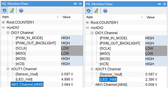
ADIO submodules viewed and controlled via the HIL Plugin
HIL Plugin with power measurement
Alternatively, if the ADIO AIN channels are configured to use the Power Probe, for power consumption measurement, the HIL Plugin will show the following. The AIN1. Voltage shows the voltage supplied to the target, which is measured by the AIN channel; the AIN1. Current is the current flowing through the shunt resistor, and AIN1. Power is the current power consumption of the target board. The left image depicts the power consumption of the target after the CPU is reset and stopped, and the right image depicts the power consumption measurement when CPU is running (maximum clock frequency, SPI communication running).
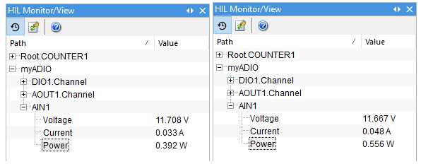
ADIO AIN channels configured to use the Power Probe
