Multi-Core Cross Connect (MCX)
In this topic:
•Time Stamp Message Generation
•Trigger Feedback to Observation Blocks
Time Stamp Message Generation
To understand the time stamping concepts of the MCDS, it is essential to understand:
•Trace messages delivered by the POBs and BOBs do not contain any timing information, i.e. there is no such thing as a time stamp within each trace message.
•Timing information is added by the MCX by adding dedicated time stamp messages.
•Whole message storage and time stamping approach is based on the underlying concept that trace data can be stored on-chip (in the Trace Memory, EMEM, LMU or TBuf) and read out by a trace tool at some later stage.
There are several time stamping concepts available, but typically either one of the following two concepts is used. For both concepts, the time stamps are derived from the counter structure.

Time Stamping Concept 1 - Ticks
The basic idea behind tick time stamps is an incremental timing information between two subsequent trace messages, by means of an 8-bit wide Tick message. A Tick message represents one MCDS clock cycle. When two subsequence trace messages are, for instance, generated, four MCDS clock cycles apart from each other, the “space” in between these trace messages is filled with “four Ticks” messages. If there is no new trace message for 255 MCDS clock cycles, then a so-called Multick is automatically generated. When a trace tools reads out the on-chip trace buffer, it can incrementally derive the exact relative time for each trace message by adding the number of MCDS clock cycles between the trace messages as defined by the number of Tick messages.
Tick based timestamp can be enabled via the Hardware, MCDS and MCX configuration dialogs as shown below.
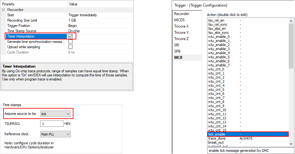
This Tick-based time stamping is the most accurate trace method (timing resolution is MCDS clock, which is typically CPU clock divided by 2), but may consume more trace buffer compared to the TSU_REL based concept described below.
The resolution of a Tick cannot be configured, i.e. it is fixed to one MCDS clock cycle.
The picture below depicts the Tick time stamp based trace timing reconstruction concept.

|
Tick-based time stamping does not support a time correlation (synchronization) of the AURIX trace to other trace sources, such as another processor or an iC7max/iC5700 BlueBox Add-on module (CAN/LIN or ADIO). |
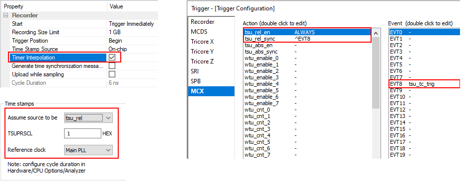
Time Stamping Concept 2 - TSU_REL
When using TSU_REL based time stamping, full 32-bit time stamps (contents of the TSUEMUCNT counter) are inserted into the trace stream/storage upon specific triggers. Such triggers can either be a periodic expiration of the TSUPRSCL prescaler (TSU_TC_TRIG) or other triggers generated by a POB or BOB and forwarded to the MCX. There are two typical use cases.
Use case 1: Periodic TSU_REL generation
The pre-scaler TSUPRSCL is used to generate a period TSU_TC_TRIG trigger. This trigger can be mapped to a MCX event and the event finally causes the action of generating a TSU_REL message (Relative Time Stamp Sync message). All trace messages, which occur in between two consecutive TSU_REL messages are interpolated (equally distributed) between the TSU_REL messages by the trace tool. Therefore, the trace timing accuracy depends on the TSU_TC_TRIG frequency. The higher the frequency the higher the timing accuracy. The highest accuracy is achieved by setting the TSUPRSCL pre-scaler value to 1.
If the TSUPRSCL value is 1 and CPU clock (also Main PLL clock) is for instance 200 MHz, this means that a TSU_REL time stamp message is generated after every 240ns. For a TSUPRSCL value of 4, this would mean a TSU_REL message every 600ns.
Below is the corresponding MCDS and MCX configuration dialog settings for this usecase.
The periodic TSU_REL time stamp based trace timing reconstruction concept is depicted in the following picture.

Use case 2: TSU_REL generation upon specific triggers
This kind of time stamp generation is not recommended.
Message Storage Control
TC2xx/TC3xx
Trace data can either be stored in the so-called Emulation Memory (EMEM) or it is streamed out via the AGBT interface. The structure of the EMEM (for a TC2xx/TC3xx emulation device) is depicted in the picture below.

The EMEM consists of three parts:
•Extended Calibration Memory (XCM)
•Trace/Calibration Memory (TCM)
•Extended Trace Memory (XTM)
The XCM is used by the calibration software of the application (i.e. CPU). It cannot be used for trace (MCDS).
The TCM can either be used by the software (CPU) or be the MCDS. The TCM is separated into so-called tiles. These tiles can be assigned to either trace or calibration. All the tiles assigned to trace form the on-chip trace buffer. The MCX manages how the trace data is written into the TCM trace buffer. The storage operation in the buffer is basically performed in two phases, the so-called Pre-Trigger Phase and the Post-Trigger Phase.
TC4x
In the case of TC4x emulation device, trace data is stored (typically) in LMU. LMU has flat address space that is divided into several regions - the actual number of them depends on the specific device. In most cases winIDEA is able to automatically configure the LMU.
The start address of trace storage must be 8B aligned. Its size can be set up to 1kB granularity.
Trigger
Pre-Trigger Phase
The storage always starts in the Pre-Trigger phase. In this phase, the MCX uses a user-defined portion of the available trace buffer (i.e. tiles assigned to trace) as a circular buffer. The size of this circular buffer is defined by the Trigger Position. It can either be:
•Begin - No circular buffer available in the Pre-Trigger phase.
•Center - Half of the trace buffer is used as a circular buffer available in the Pre-Trigger phase.
•End - The entire trace buffer is used as a circular buffer available in the Pre-Trigger phase.
Upon the occurrence of a user-defined Trigger Event, the storage operation switches into the Post-Trigger phase. This Trigger Event is either generated by the MCX itself or can originate from a Trigger-Event-Action generated by a POB or BOB.
Typical Trigger Events are:
•A CPU executes an instruction at a specific address location, such as an entry into a function.
•A CPU performs a memory write access to a specific memory address location using a specific data value. Such an event could for instance be generated by the OS signaling that a specific OS task is running.
Post-Trigger Phase
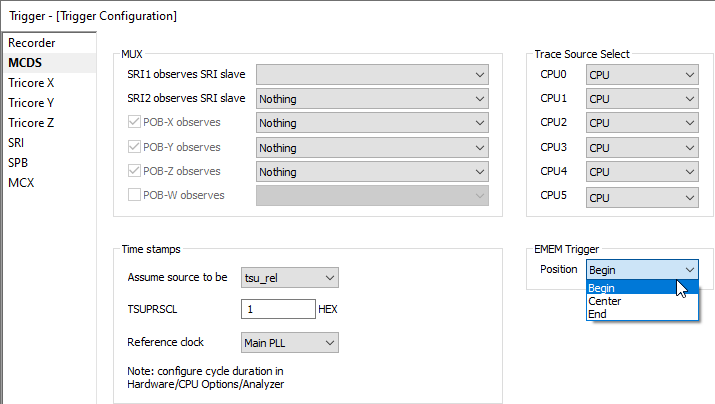
The remaining portion of the trace buffer is filled with trace messages which are generated after the occurrence of the Trigger Event (trace_done). Once the allocated trace buffer is full, trace is automatically stopped (the CPU operation is not influenced).The picture below shows the EMEM Trigger Position configuration dialog in the MCDS page.

EMEM Trigger Position
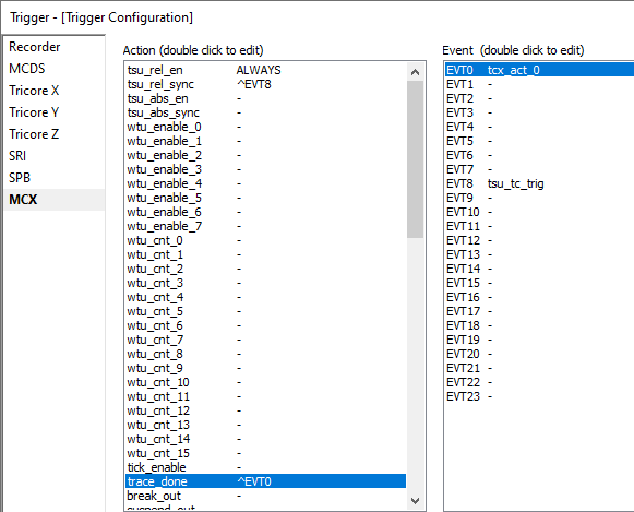
Sample trace_done Trigger Event Configuration (switch from Pre- to Post-Trigger mode upon occurrence of MCX EVT0, imported from POB X).
Event Counters
The MCX implements a set of event counters. These counters can be incremented, decremented and cleared upon input events, selectable from a pool of events. Such events may be “core instruction executed”, “cache hit” or events imported to other MCDS components such as POBs or BOBs. The event counter can either use a trigger course of MCX events or may be output via the Watchpoint Trace Unit (WTU).
Trigger Feedback to Observation Blocks
Events of the MCX may be exported and routed to observation blocks such as POBs or BOBs, where they can be used as triggers. For example, program trace of a POBs could be enabled when an event counter of the MCX exceeds a certain threshold.