NXP LPC
In this topic:
•CPU clock and Flash programming
•LPC11A02/04 Debug Pin Remapping in Boot
•Criterion for valid user code
•LPC1xxx: Read protection (CRP) area at 0x2FC
•Configuring trace pins for parallel trace
General
The debugger programs the code directly into the internal flash memory through the standard debug download. Based on the selected CPU the debugger identifies which code from the download file fits into the internal flash and loads it to the flash through the flash programming procedure hidden to the user. The flash programming procedure is implemented using NXP IAP (In-Application Programming) interface being already part of the CPU Flash Boot Loader firmware. All other code allocated outside of the flash boundaries is downloaded to the target through standard the memory writes.
|
Proper target CPU must be selected in the Debug / Configure Session dialog since corresponding flash programming procedure is selected based on the selected CPU. |

|
IAP commands use 32-bytes of space in the top portion of the on-chip RAM for execution. The user program should not use this space. |
Download verify exclusion
Due to the CPU requirements winIDEA extracts the necessary interrupt vectors from the download file before programming a 32-bit value to the 0x1C address, makes the 2’s complement of the check-sum of these vectors and programs the calculated value to the 0x1C address. This yields the CPU starting from the user code after the reset.
Consequentially when Verify is configured it’s executed after the debug download and the user would normally get error at address 0x1C since the programmed value doesn’t match with the one in the download file. The user can ignore this error or adjust his download file in a way that a 32-bit value at the address 0x1C contains proper value, which results in the CPU start executing the user code after the reset.
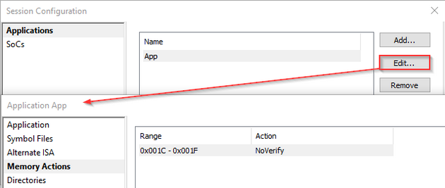
The alternative is also to skip verifying 4 bytes at address 0x1C. Picture shows the necessary setting in the Memory Actions dialog.
1. Open Debug menu / Configure Session / Applications / Memory Actions.
2. Add a Range to skip.
|
Code Read Protection (CRP)
Code Read Protection is a mechanism that allows user to enable different levels of security in the system so that access to the on-chip flash and use of the ISP can be restricted. When needed, CRP is invoked by programming a specific pattern in flash location at 0x000002FC. If value 0x12345678 is programmed to the address 0x2FC (CRP1), access to chip via the JTAG pins is disabled, which means debugger can no longer have control over the CPU via the JTAG debug interface. Hence, use code read protection with caution.
CPU clock and Flash programming
Since most of Cortex-M LPC devices need CPU clock to correctly program flash memory, you must take care to correctly set the option for CPU clock.
LPC11A02/04 Debug Pin Remapping in Boot
For WLCSP packages only: The boot loader changes the default pin configuration from reset values to the following pin functions:
•PIO0_2 register: default pin function configured as SWCLK.
•PIO0_3 register: default pin function configured as SWDIO.
•TCK_PIO0_5 register: default pin function configured as PIO0_5.
•SWDIO_PIO0_10 register: default pin function configured as PIO0_10.
PIO0_2 and PIO0_3 should be connected to debug connector and used for debugging.
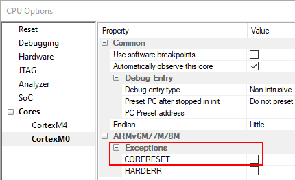
Reset vector catch
Always leave CORERESET exception unchecked in Hardware menu / CPU Options / CORE0 page.
When CORERESET is enabled, the CPU will be stopped before boot remaps debug pins and debug session will not be initialized successfully.
 |
Boot and Memory Remapping
On Cortex-M devices from LPC family a Boot Rom is present with code that is executed on reset and a memory mapping register (MEMMAP, SYSMEMREMAP). In winIDEA version 9.12.178 a following change of handling session initialization and memory remapping was introduced.
After debug connection is established the target CPU is released from reset and stopped at beginning of boot code. Initial stack pointer and reset vector is read from flash. Breakpoint is set on initial reset vector from flash. At this point CPU is ran and boot is executed. When CPU hits the breakpoint it is stopped. If the flash does not contain valid reset vector CPU is stopped with delay. Flash is then mapped to address 0x00000000 and initial stack pointer and reset vector are loaded to R13 and R15 registers respectively. User finds the CPU in this state.
Initialization script can be used if mapping RAM to beginning of memory space is desired after reset.
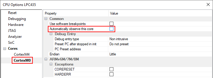
Per LPC435x specification, Cortex-M0 is not accessible through the SWD debug interface. It’s accessible only through the JTAG debug interface.
|
It’s recommended to use the JTAG debug interface when debugging LPC435x, which allows debugging both cores Cortex-M4 and Cortex-M0. |
When only SWD debug interface is available on the target debug connector, Cortex-M4 can be debugged only. Uncheck the Automatically observe this core option (checked by default) for Cortex-M0 in Hardware / CPU Options / Cores. Without this adjustment, winIDEA becomes unresponsive trying to connect to Cortex-M0 core.
 |
The flash boot loader code is executed every time the part is powered on or reset. The loader can execute the ISP command handler or the user application code. A LOW level after reset at pin P2.10 is considered an external hardware request to start the ISP command handler. Assuming that power supply pins are on their nominal levels when the rising edge on RESET pin is generated, it may take up to 3 ms before P2.10 is sampled and the decision on whether to continue with user code or ISP handler is made. If P2.10 is sampled low and the watchdog overflow flag is set, the external hardware request to start the ISP command handler is ignored. If there is no request for the ISP command handler execution (P2.10 is sampled HIGH after reset), a search is made for a valid user program. If a valid user program is found then the execution control is transferred to it. If a valid user program is not found, the auto-baud routine is invoked.
Pin P2.10 is used as a hardware request signal for ISP and therefore requires special attention. Since P2.10 is in high impedance mode after reset, it is important that the user provides external hardware (a pull-up resistor or other device) to put the pin in a defined state. Otherwise unintended entry into ISP mode may occur.
When ISP mode is entered after a power on reset, the IRC and PLL are used to generate the CCLK of 14.748 MHz.
Criterion for valid user code
The reserved Cortex-M exception vector location 7 (offset 0x 001C in the vector table) should contain the 2’s complement of the check-sum of table entries 0 through 6. This causes the checksum of the first 8 table entries to be 0. The boot loader code checksums the first 8 locations in sector 0 of the flash. If the result is 0, then execution control is transferred to the user code.
If the signature is not valid, the auto-baud routine synchronizes with the host via serial port 0.
LPC13xx Startup
The flash boot loader code is executed every time the part is powered on or reset. The loader can execute the ISP command handler or the user application code, or in case of LPC13xx it can obtain the boot image as an attached MSC device through USB. A LOW level during reset at pin PIO0_1 is considered an external hardware request to start the ISP command handler or the USB device enumeration without checking for a valid user code first. The state of PIO0_3 determines whether the UART or USB interface will be used (refer to CPU user manual for more details).
Assuming that power supply pins are on their nominal levels when the rising edge on RESET pin is generated, it may take up to 3 ms before PIO0_1 is sampled and the decision on whether to continue with user code or ISP handler/USB is made. If PIO0_1 is sampled low and the watchdog overflow flag is set, the external hardware request to start the ISP command handler is ignored. If there is no request for the ISP command handler execution (PIO0_1 is sampled HIGH after reset), a search is made for a valid user program. If a valid user program is found then the execution control is transferred to it. If a valid user program is not found, the auto-baud routine is invoked.
Pin PIO0_1 is used as a hardware request signal for ISP UART/USB and requires special attention. Since PIO0_1 is in high impedance mode after reset, it is important that the user provides external hardware (a pull-up resistor or other device) to put the pin in a defined state. Otherwise unintended entry into ISP mode may occur.
|
The sampling of pin PIO0_1 can be disabled through programming flash location 0x0000 02FC. |
The reserved Cortex-M exception vector location 7 (offset 0x 001C in the vector table) should contain the 2’s complement of the check-sum of table entries 0 through 6. This causes the checksum of the first 8 table entries to be 0. The boot loader code checksums the first 8 locations in sector 0 of the flash. If the result is 0, then execution control is transferred to the user code.
If the signature is not valid, the auto-baud routine synchronizes with the host via serial port 0 or boots from the USB port (PIO0_3 is sampled high).
Watchdog
Regular reset cannot be used with LPC devices. For more information about reset modes see Reset section. This results in short core run before it is stopped. In that time the watchdog might get enabled. It remains counting in stop mode and it is only disabled on external reset or overflow reset. Another external reset cannot be used – it would cause endless loop. Instead the watchdog status is checked after each reset. If watchdog is enabled the debug session is paused until the overflow reset is detected. Since the core is set to stop on reset the debug initialization can continue.
|
NXP advises the use of the interrupt watchdog mode while debugging. |
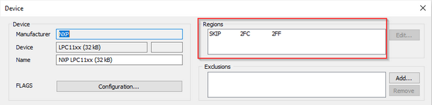
LPC1xxx: Read protection (CRP) area at 0x2FC
NXP Cortex-M LPC1xxx devices contain code read protection (CRP) area at 0x2FC. Write access to this area is skipped by default as the chip can be locked permanently, if CRP2 or CRP3 pattern is programmed incorrectly.
1. Open Hardware / <device name> / Configure.
2. See the Regions section in the Device dialog.
|
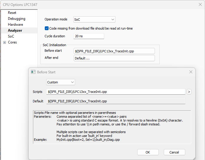
Configuring trace pins for parallel trace
Add a TraceInit script to Hardware / CPU Options / Analyzer/ SoC Initialization / Before Start page.
LPC15xx: SWO trace
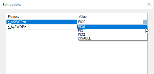
On LPC15xx devices you can configure I/O pin to use for a SWO trace. Take special care to correctly select a pin that is not otherwise used by application. SWO GPIO configuration is performed by initialization script. It is entered as a parameter to LPC15xx_TraceInit.cpp script in the CPU Options / Analyzer dialog.
|
Environment will remap selected pin to output SWO trace, disabling any function previously assigned by application. |
1. Follow Custom Configuration procedure.
2. Add the script LPC15xx_TraceInit.cpp.
3. Specify which port to use for parallel trace. Default settings:
•g_eSWOPort=PIO0
•bySWOPin=8
 |