Cypress Traveo II
In this topic:
•Debug freezing initialization scripts
Work Flash
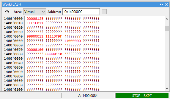
Work Flash is a flash memory used to store data (code storage for user application execution and local data storage/update for MCU-based systems). Work Flash is a part of the eCT Flash. Reading from a Work Flash that is still in an erased state will result in random data in the Memory Window. Example below.
Normal usage of work flash is as follows:
1. Erase the entire sector via the Mass Erase option.
2. Program word(s) including ECC bits.
3. Read 32-bit word including ECC.
For more information about Work Flash refer to Traveo II Family Architecture Technical Reference Manual.
Supervisory Flash (SFLASH)
|
To troubleshoot possible issues with Cypress Traveo II use logging via Help | Support | Log, enable activity (27) EVE, reset the application and inspect data in the Progress window. |
|
We highly advise to enable modification of SFLASH in winIDEA only when needed, and disable it right after they are done with changes, because there is mostly HW/SoC/boot configuration present which affects behavior of SoC. For example, JTAG access can be locked and it cannot be used again. |

Programming of Supervisory Flash is divided to two types of programming:
•User rows (available in VIRGIN and NORMAL state of SoC) and
•Cypress rows (available only in VIRGIN state of SoC).
Program User rows
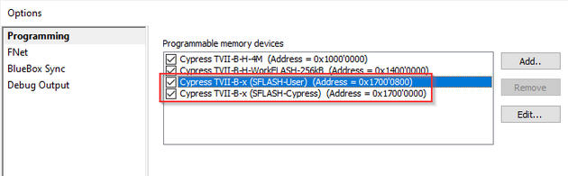
This portion of flash can be modified if the device is in either VIRGIN or NORMAL state. To enable programming SFLASH follow these steps:
1. Open Hardware | Options | Programming.
2. Select the programmable memory devices.
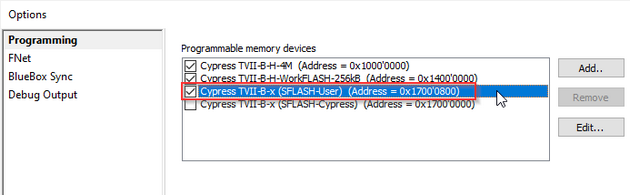
Editing SFLASH-User
You can edit SFLASH-User via:
•Target Download (recommended)
•Regular Download (not recommended, since user can forget this download file checked in download list and then it will be programmed over and over again upon every Ctrl+F3, which is generally bad for such sensitive flashes)
Program Cypress rows
This portion of flash can be modified if the device is in VIRGIN.
|
It is recommended to be changed only by Cypress. These portions of flash are in winIDEA for security reasons shown as separate flash. |
Note that flash operation is same from user perspective as for user rows.
1. Open Hardware | Options | Programming.
2. Select the programmable memory devices.
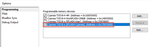
Editing SFLASH-Cypress
You can edit SFLASH-User via:
•Target Download (recommended).
•Regular Download (not recommended, since user can forget this download file checked in download list and then it will be programmed over and over again upon every Ctrl+F3, which is generally bad for such sensitive flashes).
Updating device boot
This is a specific use case - a recommended procedure for updating device boot. To enable SFLASH, update boot files and perform Target Download follow these steps:
1. Open Hardware | Options | Programming.
2. Enable SFLASH-User device.
3. Enable SFLASH-Cypress device.
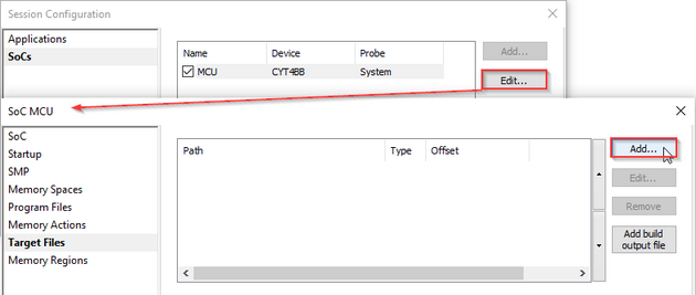
4. Open Debug | Configure Session | SoCs | Edit | Target Files.
5. Add provided boot update files by clicking the Add button.
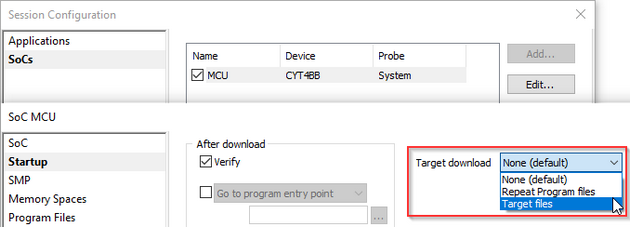
6. Open Debug | Configure Session | SoCs | Edit | Startup.
7. Make sure the option Target files in selected.
8. Perform Target download via Debug | Target Download | <appropriate file>.
Cache Write-through scripts
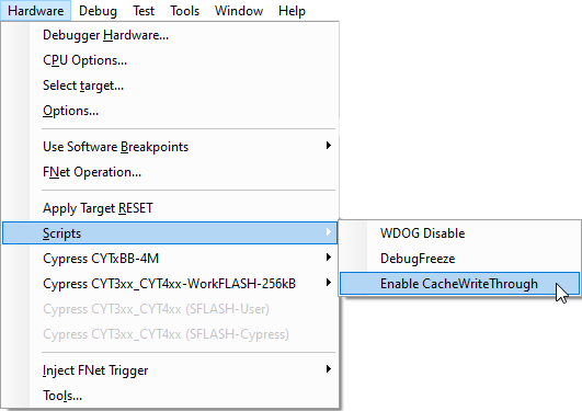
In general for a real-time observation of the variables these must be written in the data memory and not for example only held in the cache since cache memory is not visible to the debugger. If you want the "cached only" variables to be seen to debugger, use the provided L1 Cache Write-through enable EVE script, which configures the microcontroller to propagate writes of variables cached in the L1 cache also to the memory.
The script sets the FORCEWT bit of the CM7_CACR register. The debugger has no access to the contents of the cache memory, the only way to observe it's contents by debugger is by forcing it to write-through any changes directly from the cache memory to the SRAM locations, which are accessible by debugger.
Example below shows how variables are seen to debugger in the memory:
Without Write-through |
With Write-through |
||
|---|---|---|---|
Cache value |
Memory value |
Cache value |
Memory value |
0x00000000 |
0x000000E7 |
0x00000000 |
0x00000000 |
0x00000001 |
0x000000E7 |
0x00000001 |
0x00000001 |
0x00000002 |
0x000000E7 |
0x00000002 |
0x00000002 |
The script is accessible in Hardware | Scripts | Enable CacheWriteThrough. Its execution is called on a explicit request. Do note that its effect is reset if the microcontroller goes through any kind of a reset and the variables being cached only will no longer be visible in the real-time Watch Window.
Debug freezing initialization scripts
Use these scripts (<device>_DebugFreezeEnable.cpp) for a better synched Run/Stop mechanism. Supported on the following devices:
•CYT4DN •CYT4BF •CYT4BB •CYT3DL •CYT3BB |
•CYT2BL •CYT2B9 •CYT2B7 •CYT2B6 |
|
These scripts use CTM/CTI Channel 2 and should not be used together with the Trace Cross Trigger Channel CTM/CTI, because they may interfere with trace. A warning is added to the Progress window: Warning! Disable this initialization script if trace is used. Debug freeze trigger shares the CTM channel 2 with the Trace trigger. |
Debug session initialization prerequisites
By default Traveo II device requires debug interface operating at frequency higher than 1.5 MHz. This permits the debugger to execute the necessary debug initialization procedures fast enough and within the device start up time window constraint, after the CPU reset line is released by the BlueBox.
When debug interface:
•SWD Debug Protocol is used, set SWD clock to 1500 kHz or higher
•JTAG Debug Protocol is used, set JTAG scan speed to 1500 kHz or higher
While connecting to the CPU, winIDEA reports a warning if the debug interface frequency is not configured properly.
When the application is properly linked and programmed into the FLASH, the CPU stops after reset at the address to which the reset vector points to. If FLASH contains no valid code (e.g. empty device), the CPU stops in boot code.
|
On all Cypress Traveo II devices, use the Regular RESET method for reset in initialization operation. |
Set SWD and JTAG clock
1. Open Hardware | CPU Options | SoC.
2. Select the SWD Debug Protocol.
3. Set the SWD clock to 1500 kHz or higher and confirm.
4. Open the JTAG page.
4. Set JTAG Debug Protocol to 1500 kHz or higher and confirm.
Initialize Debug session via EVE script parameter
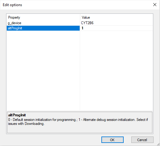
winIDEA enables alternate debug session initialization if issues with downloading occur. It will only affect the download operations. Follow Custom Configuration procedure and select "1" in the altProgInit field.
Cypress Traveo Emulation Adapters
Cypress Traveo II packages have different trace capabilities. For the 64-pin, 80-pin and 100-pin packages Emulation Adapter Cypress Traveo II CYT2B9 and Emulation Adapter Cypress Traveo II CYT2B7 provide the trace interfaces, where trace port is not available or lacks the full trace capability.
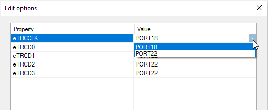
By default, P18 port pins (P18_3 – P18_7) or P22 port pins (P22_0 – P22_4) are set as GPIO pins. To configure these pins as trace pins in winIDEA, open the CPU Options | Analyzer.
TRACE CLOCK and TRACE DATAn signals can be allocated either to IO port P18 or IO port P22. Typically, an embedded target will have all trace signals connected either to P18 or P22. However, it’s also possible to mix these signals across both ports randomly. Just for example: TRACE CLOCK, TRACE DATA1, TRACE DATA3 signals on P18 and TRACE DATA0, TRACE DATA2 on P22.
1. Follow the Custom Configuration procedure.
2. Add the script CYT2Bx_TraceInit.cpp.
3. Depending on the user target board configuration allocate:
•TRACE CLOCK Port to PORT 18 (or PORT 22).
•TRACE DATAn PORT to PORT 18 (or PORT 22).
4. Enable 2, 3 for Trace Trigger and Flush in Use Cross Trigger Channels in Hardware | CPU Options | SoC.